webinar banner AI 2026 v2

How to multiply currents: Inside a Counterfeit Analog Multiplier

How to multiply currents: Inside a Counterfeit Analog Multiplier
by Ken Shirriff on 09-27-2020 at 10:00 am

Inside a Counterfeit Analog Multiplier

A recent Twitter thread about a counterfeit analog multiplier chip attracted my attention since I’m interested in both counterfeit integrated circuits and how analog computers multiply. In the thread, John McMaster decapped a suspicious AD633 analog multiplier chip and found an entirely different Rockwell RC4200 die inside. Why would someone do this? Probably because the RC4200 (1978) currently sells for about 85 cents, while the more modern laser-trimmed1 AD633 (1989) sells for about $7.2

Die of the RC4200 analog multiplier with functional blocks labeled. Die photo courtesy of John McMaster.


Analog multiplication

Analog multiplication has many uses such as mixers, modulators, and phase detectors, but analog computers are how I encountered analog multiplication. A typical analog computer uses voltages to represent values and is wired up through a plugboard to solve a particular equation. Adding or subtracting two values is easy with an op amp, as is multiplying by a constant. Integration seems like it would be difficult, but it’s almost trivial with a capacitor; analog computers excelled at solving differential equations.

Multiplying two values, however, was surprisingly difficult; multiplication techniques were slow, inaccurate, noisy, or expensive. One accurate but slow multiplier used the Rube-Goldberg configuration of servo motors turning potentiometers.3 A 1969 multiplier circuit uses a light bulb and photocells. A fast and accurate approach was the “parabolic multiplier”, built from numerous expensive high-precision resistors.4 The approach I’ll discuss is to multiply by adding the logarithms and taking the exponential. Inconveniently, this approach magnifies even small differences between the transistors. It is also very sensitive to temperature. As a result, this approach was simple but inaccurate.

The Model 240 analog computer from Simulators, Inc. includes analog multipliers using the parabolic multiplier approach.


However, the development of analog integrated circuits created new opportunities for analog multiplication circuits. In particular, since the transistors in an integrated circuit were created together, they have nearly-identical properties. And the components on a tiny silicon die are all at nearly the same temperature.5

The first analog multiplier integrated circuit I could find is a television demodulator from 1967. The Gilbert cell technique was introduced by Barrie Gilbert in 1968 and is used in most analog multipliers today.6 The AD530 was introduced around 1970, and became an industry standard, but required external adjustments for accuracy. Laser-trimming the resistors inside the integrated circuit during manufacturing greatly improved the accuracy, an approach used in the AD633, the integrated circuit that was counterfeited.

Before explaining the circuitry of the RC4200 (the multiplier inside the counterfeit chip), I’ll discuss the components that it is constructed from, and how they appear in an integrated circuit. This will help you recognize these structures in the die photo.

Transistors

Transistors are the key components in a chip. The photo below shows an NPN transistor in the RC4200 as it appears on the chip. The different blue colors are regions of silicon that have been doped differently, forming N and P regions. The white lines are the metal layer of the chip on top of the silicon—these form the wires connecting to the emitter (E), base (B), and collector (C).

An NPN transistor on the RC4200 die. The emitter is embedded in the base, with the collector underneath.


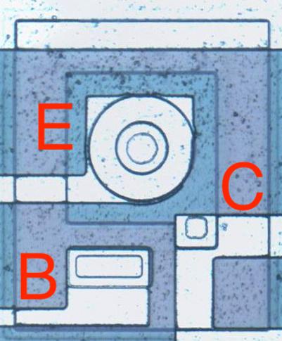
You might expect PNP transistors to be similar to NPN transistors, just swapping the roles of N and P silicon. But for a variety of reasons, PNP transistors have an entirely different construction. They consist of a circular emitter (P), surrounded by a ring-shaped base (N), which is surrounded by the collector (P). This forms a P-N-P sandwich horizontally (laterally), unlike the vertical structure of the NPN transistors. The diagram below shows one of the PNP transistors in the RC4200.

A PNP transistor has a circular structure.


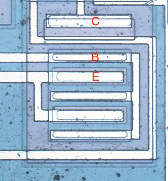
The input and output transistors in the RC4200 are larger than the other transistors and have a different structure to support higher currents. The photo below shows one of the output transistors. Note the multiple interdigitated “fingers” of the emitter and base.

A larger output transistor with parallel emitters and bases.


Capacitors

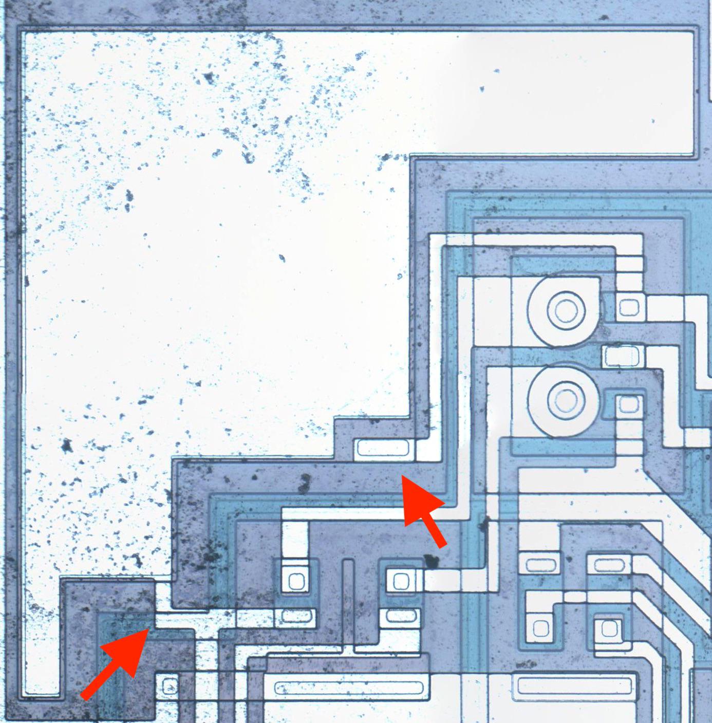
Capacitors are important in op amps to provide stability. A capacitor can be built in an integrated circuit as a large metal plate separated from the silicon by an insulating oxide layer. The main drawback of capacitors on ICs is they are physically very large. The 15pF capacitors in the RC4200 have a very small capacitance but take up a large fraction of the die area. In the photo below, the red arrows indicate the connection to the capacitor’s metal layer and to the capacitor’s underlying silicon layer.

The large metal area on the upper left is a capacitor.


Resistors

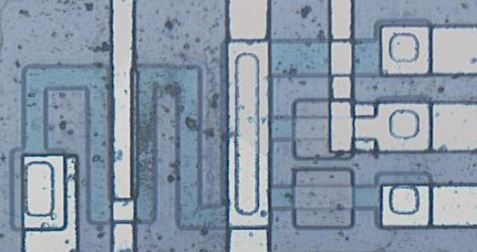
Resistors are a key component of analog chips. Unfortunately, resistors in ICs are very inaccurate; the resistances can vary by 50% from chip to chip. The photo below shows four resistors, formed using different techniques. The first resistor is the zig-zagging blue region on the left. It is formed from a strip of P silicon, with metal wiring (white) attached on the left and right. Its resistance is 3320 Ω. The resistor in the upper right is much shorter, so it is only 511Ω (long, narrow resistors have higher resistance than short, wide resistors). The remaining resistors are 20KΩ despite their small size because they are “pinch resistors”. In the pinch resistor, the square layer of brownish N silicon on top makes the conductive region much thinner (i.e. pinches it). This allows a much higher resistance for a given size. (Otherwise, a 20 KΩ resistor would be 6 times as long as the first resistor, taking up excessive space.) The tradeoff is the pinch resistor is much less accurate.

Four resistors, one on the left and three on the right.


Multiplying with logs and exponentials

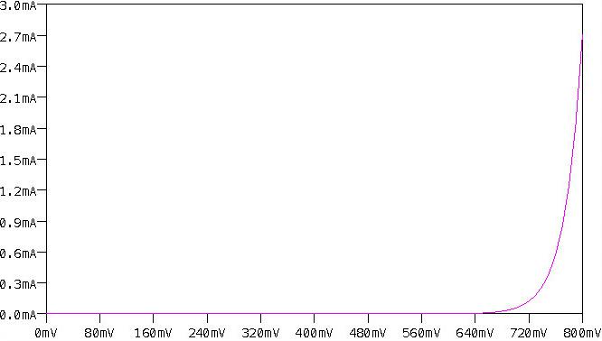
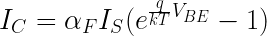
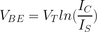
This integrated circuit multiplies using the log-antilog technique. The idea is that if you take the log of two numbers, add the logs together, and then take the antilog (i.e. exponential), you get the product of the two numbers. Conveniently, transistors have a logarithmic / exponential characteristic: the current through the transistor is an exponential of the voltage on the base. Specifically, if VBE is the voltage between the transistor’s base and emitter, the current through the collector (IC) is an exponential of that voltage, as shown in the graph below. The analog multiplier takes advantage of this property.

Ic vs Vbe curve for a transistor, showing the exponential relationship. Generated by LTspice.


The main complication with this approach is that the curve above is very sensitive to the temperature and to the manufacturing characteristics of the transistor. Because the curve is exponential, even a small shift in the curve will radically change the current. This was a serious difficulty when building a multiplier from discrete transistors, since the properties varied from transistor to transistor. To stabilize the temperature, some multipliers used a temperature-controlled oven. However, using an integrated circuit mostly solved these problems. The transistors in an integrated circuit are well-matched since they were built from the same piece of silicon under the same conditions. And the transistors in an integrated circuit die will be at almost the same temperature. Thus, integrated circuits made transistor-log circuits much more practical.

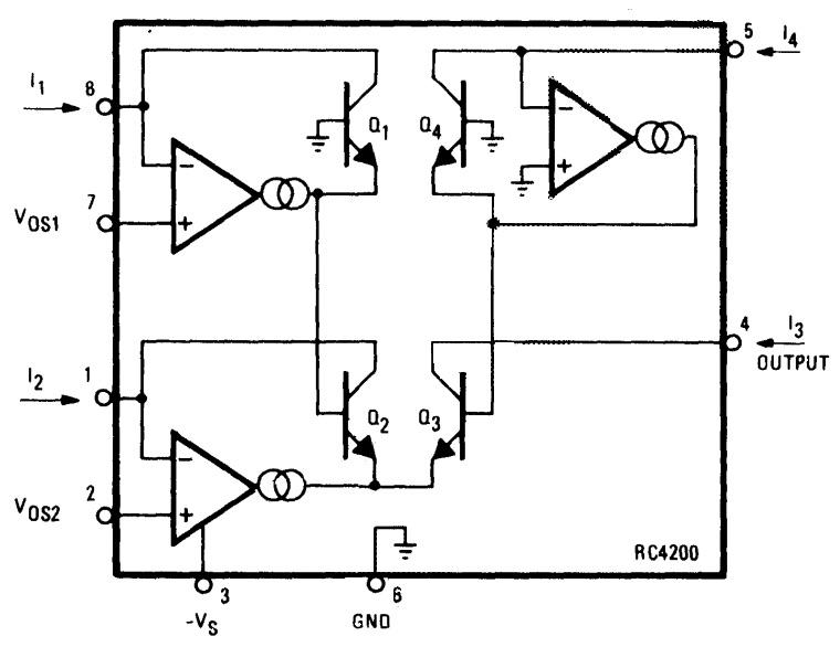
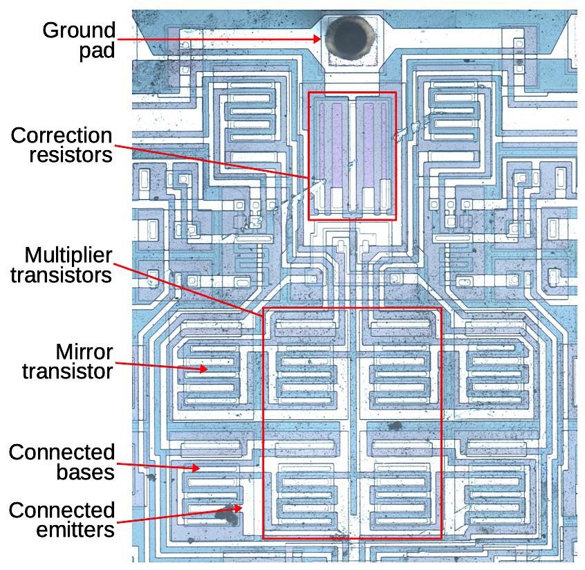
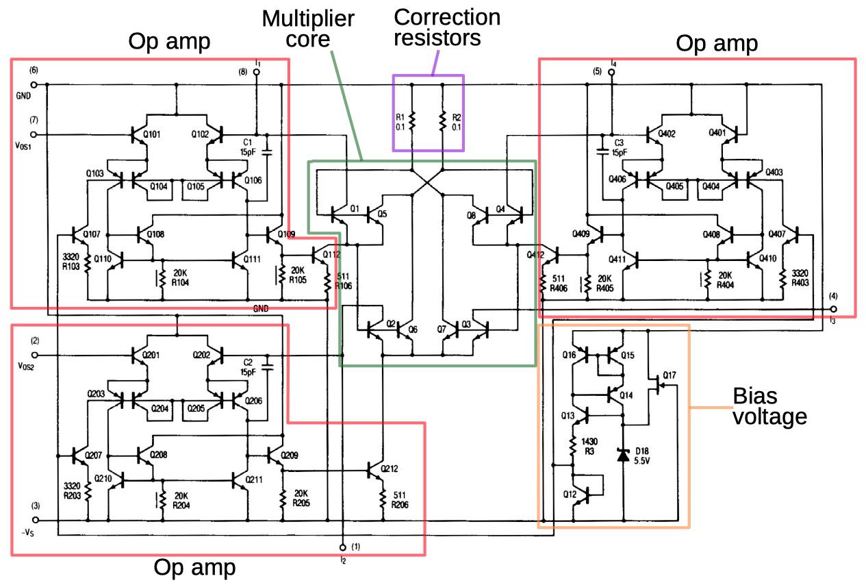
The diagram below shows the structure of the RC4200 multiplier chip. The user provides three current inputs (I1, I2, and I4) and the chip computes the output current I3, where I3 = I1×I2÷I4. (The use of current inputs and outputs is a bit inconvenient compared to other multipliers, such as the AD633, that use voltages.)

Structure of the RC4200 multiplier, from the datasheet. Note that the supply voltage (pin 3) is negative. VOS1 and VOS2 are offset adjustment pins to improve accuracy.


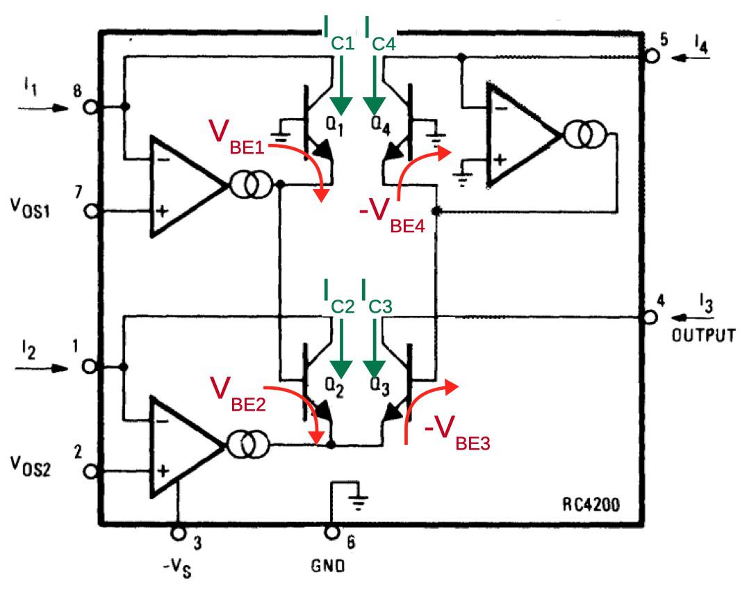
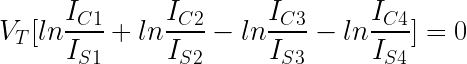
The four transistors in the middle of the diagram are the multiplier core, the key to the IC’s operation. The transistors are configured so their base-emitter voltages sum: VBE3 = VBE1+VBE2-VBE4. Because the transistor current is related exponentially to the voltage, the result is that I3 = I1×I2÷I4.

In more detail, first note that the voltages VBE1 through VBE4 control the collector currents IC1 through IC4 through the transistors (below). The op amps adjust the base-emitter voltages so the input currents match the transistor currents, i.e. I1 = IC1 and so forth. (This is accomplished by op amp feedback.) Now, if you go through the loop of base-emitter voltages starting at the base of Q1 and ending at the base of Q4 (red arrows), you find that VBE1+VBE2-VBE3-VBE4 = 0. (The voltages must sum to zero since you start at ground and end at ground.7) Now, because IC is related to exp(VBE), taking the exponential of the equation yields IC1×IC2÷IC3÷IC4 = 1. (Details in footnote8.)

Traveling around the loop indicated by the arrows, the voltages must sum to 0.


Next, I’ll explain how the VBE voltages are generated. Each current input has an op amp associated with it that produces the “correct” VBE voltage for the current using a feedback loop9 For example, suppose IC is too low so not all the input current flows through the transistor. The excess current will raise the voltage on the op amp’s negative input, causing it to reduce its output voltage and thus the transistor’s emitter voltage. This raises VBE (since the base will now be higher compared to the emitter), causing more collector current to flow through the transistor. Similarly, if too much current is flowing through the transistor, the op amp’s input will be pulled lower, reducing VBE. Thus, the feedback loop causes the op amp to find the exact VBE for the current input.10

Correcting for emitter resistance

The above circuit works reasonably well, but there’s a complication: the transistors have a small emitter resistance R. The voltage drop across this resistance will increase VBE by ICR, disturbing the nice exponential behavior. This creates a nonlinearity that reduces the accuracy of the result. The datasheet says that “Raytheon has developed a unique and proprietary means of inherently compensating for this undesired term.” They don’t explain this further, but by studying the die I have figured out how it works.

In the compensation circuit, each of the four multiplier transistors is paired with an identical “mirror” transistor with the corresponding emitters and corresponding bases connected, as shown below. These connections give the paired transistors the same base and emitter voltages, so they have the same collector currents. In other words, they form a current mirror. The mirrored currents are fed into special correction resistors that match the undesired emitter resistance, 0.1 Ω according to the datasheet.11 The voltage across the correction resistors will be the same as the excess voltage that needs to be compensated (since the resistance and current are the same). The final step is the correction resistors are connected to the base of the multiplication transistors, replacing the connection to ground. This will shrink VBE by the amount it was erroneously increased, fixing the computation.

The main multiplier consists of four transistors. Each transistor has a mirror transistor generating the same current, used to correct for emitter resistance.


Why are there two correction resistors? Recall that the multiplier has two transistors adding and two transistors subtracting (i.e. VBE1+VBE2-VBE3-VBE4 = 0). To handle this, the correction circuit is split in two. The left half sums IC1 and IC2 and applies this current to a correction resistor on the Q3/Q4 side, while the right half sums IC3 and IC4 and applies this to a correction resistor on the Q1/Q2 side. The addition and subtraction work out to yield the desired net correction.

Schematic

The schematic below shows the complete circuitry of the RC4200; I’ve highlighted the main functional blocks. (Inconveniently, I didn’t find this schematic until after I’d traced out the circuitry from the die photo.) The multiplier core and the correction resistors were discussed above The op amps circuits are fairly similar to the 741 op amp, which I’ve written about. They lack the output stage of typical op amps; the output transistor (Q112/Q212/Q412) corresponds to the intermediate gain state in a typical op amp. The bias circuit (orange, lower right) provides a fixed bias voltage for the op amps.12

Schematic from the datasheet, with main functional groups labeled.

Conclusion

Before integrated circuits, analog multiplication was difficult to implement. However, integrated circuits made it easy to create matched transistors, leading to fast, inexpensive analog multiplication integrated circuits. Unfortunately, analog multiplier integrated circuits were introduced just as analog computers were dying out, killed by inexpensive digital microprocessors, so analog computing missed most of the benefit of these chips.

While most analog multipliers use a circuit called the Gilbert cell, the Raytheon RC4200 analog multiplier uses a different technique to multiply and divide values represented by currents. Although, it includes a special error compensation circuit to improve its accuracy, it is obsolete compared to accurate, laser-trimmed multipliers. Now, counterfeiters re-label RC4200 chips and sell them as the more-expensive AD633 multiplier.

Die photo of the RC4200, courtesy of John McMaster.


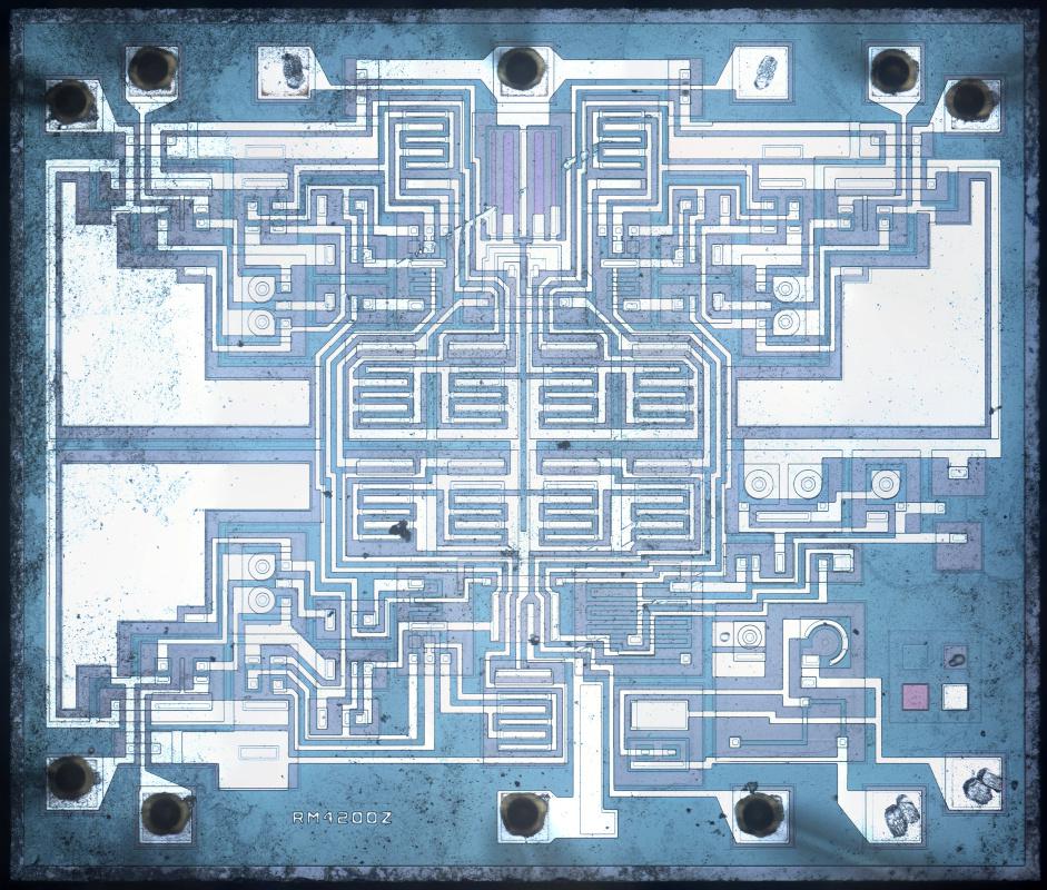
I announce my latest blog posts on Twitter, so follow me at kenshirriff for updates. I also have an RSS feed. Thank you to John McMaster for the die photos used in this blog post; the photos are here.

Notes and references

  1. One reason that the AD633 multiplier is so expensive is that the resistors on the die are laser-trimmed resistors for accuracy. To get an accurate result, an analog multiplier requires exactly-tuned resistances. The older RC4200 requires adjustable external resistors, which is much less convenient. 
  2. I’m a bit puzzled by this counterfeit chip. Sometimes people will label a cheap op amp as an expensive op amp, as explained by Zeptobars. At first glance, that’s what’s going on here: a cheap multiplier repackaged as an expensive one. However, the two multipilers are so different that I can’t imagine one working at all in place of the other. Specifically, the AD633 takes differential voltage inputs and outputs two currents (a differential current), and it computes A×B+C. The RC4200, on the other hand, takes current inputs and outputs a single current, and it computes A×B÷C. 
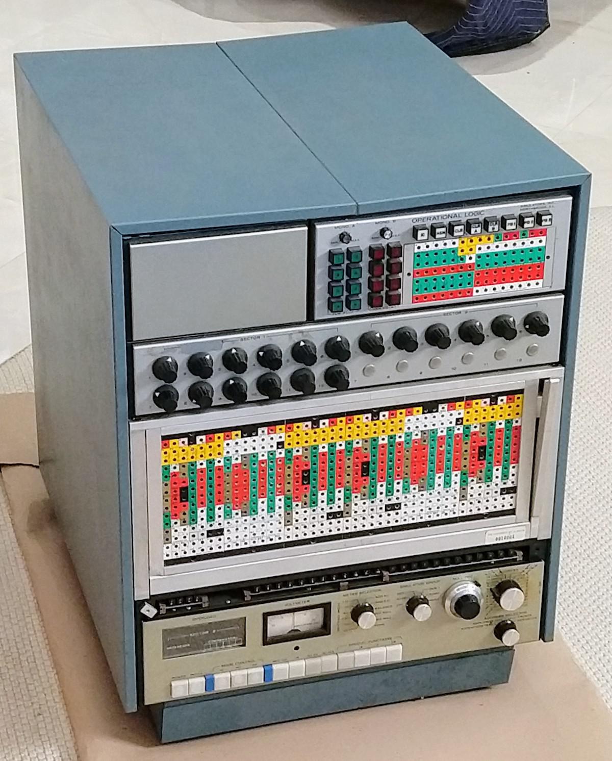
  3. An example of a servo multiplier is the Solartron Servo Multiplier from the late 1950s. This 17-pound unit contained a potentiometer controlled by a servo motor, allowing it to multiply numbers represented by +/- 100 volts. It’s surprisingly fast considering its mechanical operation, responding in under 30 milliseconds. Power consumption was high: 70 watts, cooled by a fan. (In comparison, the RC4200 chip uses 40 milliwatts of power.)
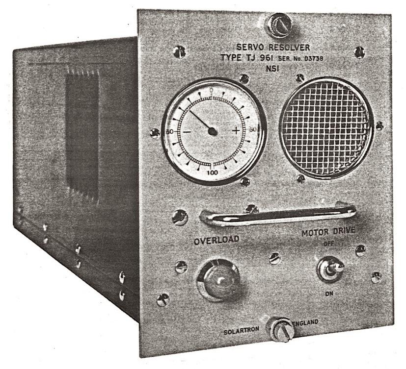
    This photo shows the Solartron TJ961 Servo Resolver. This implements multiplication as well as sine/cosine computation. Photo from manual via Analog Museum.


  4. The 1969 analog computer I’m restoring uses a parabolic multiplier, a technique used for high-accuracy multiplication. The idea is that to compute A×B, you compute ((A+B)^2 – (A-B)^2)/4, which has the same value. That equation looks much more complex than the original product, but is easier to implement on an analog computer because op amps can perform the sums, subtraction, and division by four. Squaring is easier than multiplication because it is a function of a single variable, so it can be implemented by an “arbitrary function generator”.
    Parabolic multiplier circuit board from a Simulators, Inc. 2400 analog computer.


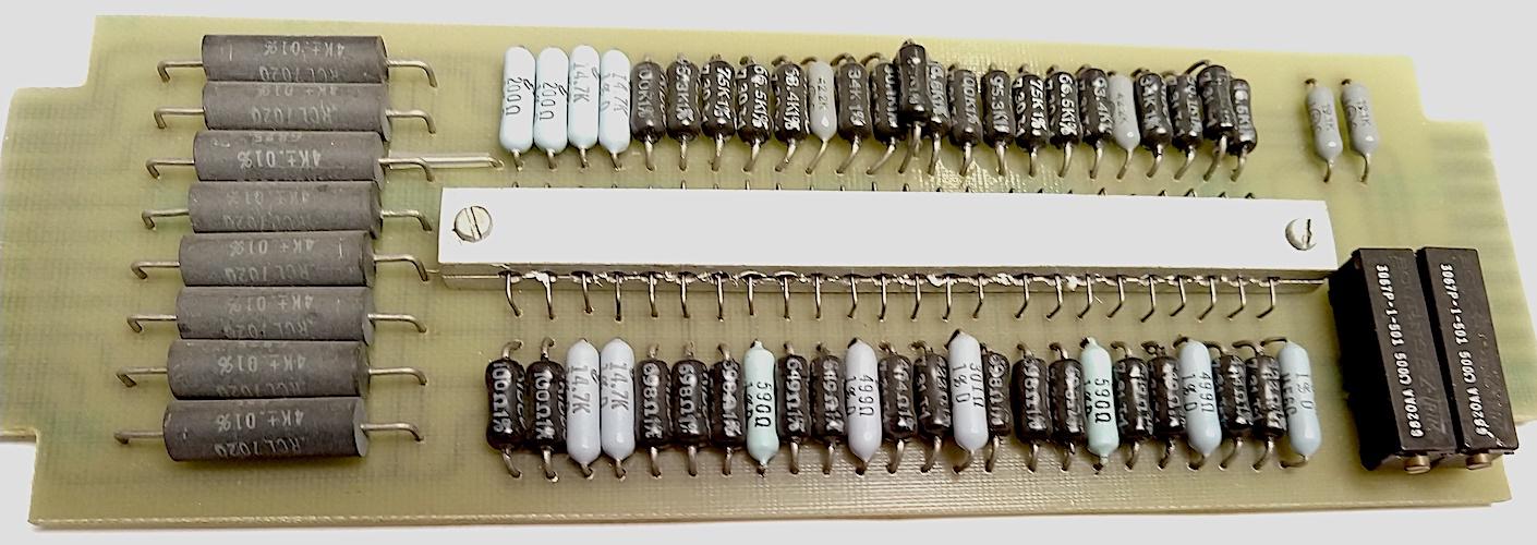
    The photo above shows a function board from an analog computer that computes the square, i.e. a parabola. The board approximates the function by multiple piecewise-linear segments, each defined by resistors. (Note the extremely accurate 0.01% resistors on the left.) The metal block in the center holds diodes, temperature-balanced by the metal. Each diode is biased to turn on at a particular voltage; the diodes act as switches, selecting the appropriate resistors for each linear segment. Note the large amount of precision hardware required for multiplication; a single product requires two of these parabolic function boards as well as multiple op amps. 

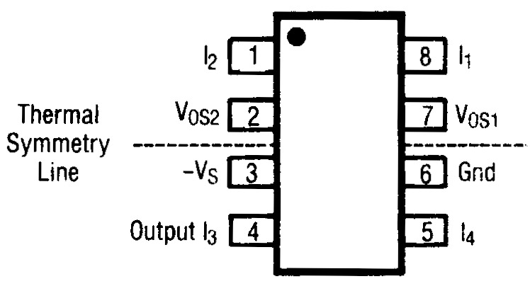
  5. To minimize the effect of temperature on the integrated circuit, the critical multiplier transistors are placed close together in the center of the chip. If there is a thermal gradient across the chip, this will minimize the temperature difference between the transistors. (Compared to putting the transistors in the corners, for instance.) To reduce temperature gradients even more, the datasheet specifies a “thermal symmetry line”. Putting a temperature source on this line ensures that the hotter transistors will tend to cancel each other out.
    The datasheet shows the IC’s thermal symmetry line.


  6. Barrie Gilbert, inventor of the Gilbert cell, has a video explaining translinear circuit, circuits based on the exponential current-voltage relationship of a bipolar transistor. This video explains translinear analog multipliers in detail, discussing two approaches> The first approach, used by the RC4200, is the “log-antilog” approach, where op-amps force and sense the collector currents. The second, used in the AD633 and many other multipliers, is the “integrated” approach, built from voltage-to-current conversion, a differential current-mode core, and current-to-voltage conversion. 
  7. I should mention that the chip uses a -15 V supply, so ground is the highest voltage and the other internal voltages are all negative. Just a warning since this makes things confusing and backward compared to circuits where ground is the low voltage. 
  8. The relationship between the base voltage and the collector current is given by the Ebers-Moll model. This equation (below) is filled with interesting constants: α: a gain factor (almost 1), k: the Boltzmann constant, IS: the saturation current (extremely small, order of 10-15 A), T: the absolute temperature, q: the charge on the electron. (The temperature in the exponential term reflects the importance of temperature stability for the multiplier.)


    Substituting the thermal voltage VT (about 26 mV) for kT/q, making some minor approximations, and taking the log yields:


    Substituting that into the multiplier’s VBE loop equation yields


    Taking the exponential and assuming the transistors all have the same temperature and saturation current yields the desired equation relating the four currents:


    This equation shows how the four currents are related by multiplication and division. See the datasheet for more details. 

  9. In a sense, the op amps compute the inverse of the transistor’s exponential function. The transistor takes VBE as an input and produces the exponential current as an output. However, we have the current as the input and want the logarithmic voltage as the output. By using the op amp with a function in its feedback loop, we can find the inverse of a function, in this case giving us the logarithm. That is, the op amp will converge on the output X where f(X) equals the input, i.e. X = f-1</sup(input). The same technique can be used to generate a square root from a multiplier chip: use the multiplier to square its input, and then use an op amp to compute the inverse function, i.e. the square root. 
  10. You might wonder why the op amp finds the “correct” value and doesn’t overshoot and oscillate. Handwaving away all the theory, the idea is that the capacitor on the op amp input stabilizes it and prevents oscillation. Even so, the datasheet warns that the circuits become unstable as the input currents approach 0. This corresponds to dividing by zero, so it’s not surprising that the circuitry doesn’t handle it well. Mathematically, the op amp is trying to find ln(0), which isn’t going to work. If you want to multiply by zero or negative values, the datasheet describes how the inputs can be biased with resistors to keep the inputs positive but still get the correct answer. 
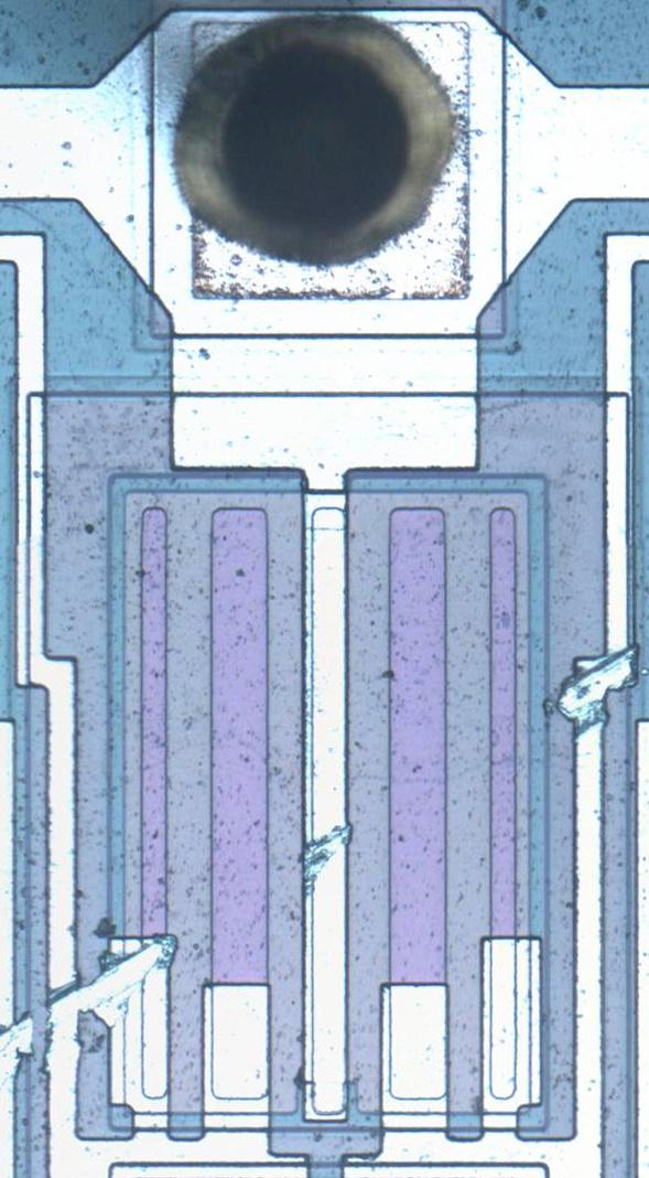
  11. The two resistors below are used for the emitter correction; they have unusual construction and a very small resistance, 0.1 Ω. Each resistor consists of the two vertical stripes, connected together at the bottom; the vertical region in the center is connected to the ground pin, forming the other side of each resistor. These resistors improve the accuracy of the product by correcting for the emitter resistances. Based on their purple color, which doesn’t appear elsewhere on the die, they appear to be specially doped. The metal contacts at the bottom cover part of the resistor; I believe that by adjusting the size of the metal contacts, the resistor values can be tuned. I believe that the thick and thin regions allow for coarse and fine tuning.
    Precise small-valued resistors provide a correction factor.


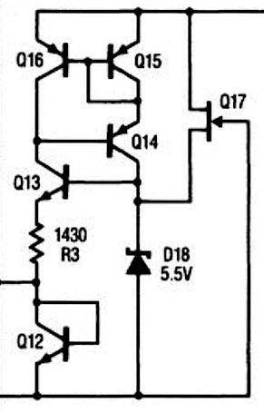
  12. The bias voltage circuit generates a stable voltage of one diode drop (about 800 mV) from Q4’s collector; this voltage biases the op amps. The tricky part is how to keep the power supply voltage from influencing this voltage or the Zener voltage.
    The bias generation circuit, from the datasheet.


    The idea is that the Zener diode puts 5.5 volts on the base of Q13. The voltage across R3 will be two diode drops lower (2.8 V) due to Q13 and Q12. This yields a fixed current of 2.8 V / 1430 Ω = 2 mA through Q4, resulting in a stable voltage drop across Q12 and a stable output. But a Zener’s voltage fluctuates a bit with current, so the clever part is how the Zener’s current is kept stable. Transistors Q14, Q15, and Q16 form a current mirror, so the current through the Zener will match the current through the resistor, which is 2 mA. Thus, the Zener voltage keeps the resistor current and output voltage stable, while the resistor current keeps the Zener stable. The final piece of the puzzle is the FET Q17, which provides a tiny current through the Zener to start the feedback cycle. 


Innovating to Survive

Innovating to Survive
by Vivek Wadhwa on 09-27-2020 at 8:00 am

Innovating to Survive

The global COVID-19 pandemic has almost shut down entire industries, forcing companies of all sizes to adapt and evolve. It has also done incredible things for a pivot to innovation.

Safety has had to come first. And for many, that meant changing how they worked, using technology to power a shift to remote work and servicing of customers. For some, like retailers, restaurants and manufacturers, it meant shutting down key services or production lines and pivoting to new offerings or entering new markets just to survive and stay relevant. Others, rather than just close doors, have repurposed their assets to contribute to the collective effort to fight the crises.

When commercial flights were shut down, airlines like Virgin Atlantic, Lufthansa, and American Airlines switched to cargo-only flights. In the UK, healthy fast-food chain Leon announced it was turning its 65 restaurants into shops, selling meals via both click-and-collect and delivery. Hotels started offering day rates for remote workers. And multiple manufacturers, like Scottish craft beer specialists BrewDog, converted their plants to produce hand sanitiser.

What does it take to shift this fast successfully? And is this kind of progress sustainable?

The reality is that it is not essential that we be thrown into crisis before this kind of change can take place.

With the enforced change in human movement and behaviour came a change in customer demand. Businesses had to think and act fast to repurpose assets, talent, resources, distribution channels, offerings. Minus the crisis, it’s what successful businesses do every day.

SpaceX’s giant step

On 11 April 2019 – before we knew what 2020 would bring – a Falcon Heavy rocket was launched Cape Canaveral, Florida, making history. It was the first in a new generation of space exploration: a rocket that would not only be able to pilot its way through space, but be able to navigate and return to Earth for re-use, radically reducing the cost of space travel.

To achieve this, SpaceX combined radical and creative funding systems, brilliant talent, and perhaps most importantly, vision. But the question at the heart of this isn’t – ‘how did SpaceX achieve this’; the question is why the incumbents didn’t? How has innovation and creativity become so stifled in large, established organisations that it takes a new kid on the block to go, quite literally, where no-one has gone before?

It’s about culture, leadership, and some very practical steps that enable businesses to be their own catalysts for change, rather than relying on a crisis to spark exponential change.

The DNA of organisations that thrive through change

From Incremental to Exponential, a book I have co-authored with Ismail Amla, looks at what it takes to drive exponential change in an enterprise. In it, we examine five common components that make up the DNA of organisations that thrive through change.

  • Firstly, speed. Leading companies just operate faster – from reviewing strategies to allocating resources. McKinsey research indicates that these companies relocate talent and capital four times more quickly than their less nimble peers.
  • Secondly, being ready to invent. While business need to maintain the profitable elements of what they do, operating at business as usual is dangerous. Leading businesses are investing as much in upgrading the core as they are on innovation.
  • Thirdly, being all-in. These companies aren’t just making decisions faster, the decisions themselves are bolder, braver and further outside of the box.
  • Fourthly, making data-driven decisions. Data is providing the fuel to power better and faster decision making. High-performing organisations are three-times more likely to say that data and analytics initiatives contribute at least 20 percent to EBIT. Which is profound.
  • And finally, following the customer. Top companies that sustain a comprehensive focus on the customer (in addition to operational improvements) have been shown to reap economic gains ranging from 20 to 50 percent of the cost base.

You’ll find a wealth of insight on what it takes for large companies to see the future and rethink innovation in From Incremental to Exponential, released in the US on October 6th.

Also, Ismail and I will be doing a series of podcasts on LinkedIn to discuss what it takes for legacy companies to reinvent themselves under the “Innovating to Survive” theme. I hope you will join us for these! 


Autonomous Vehicles: Avoiding Obstacles and Responsibility

Autonomous Vehicles: Avoiding Obstacles and Responsibility
by Roger C. Lanctot on 09-27-2020 at 6:00 am

Autonomous Vehicles Avoiding Obstacles and Responsibility

The headline screams off of the page and challenges all that we know about the fatal crash in Tempe, Ariz., that took the life of Elaine Herzberg two and a half years ago. “Backup Driver of Autonomous Uber SUV Charged with Negligent Homicide in Arizona.”

How could the National Transportation Safety Board (NTSB) associate itself with such an outcome?  Shouldn’t Uber ATG bear full responsibility for the crash?

An NPR (National Public Radio) report notes that “Rafaela Vasquez (the driver of the Uber Advanced Technologies Group car) appeared in court on Tuesday (last week) in Maricopa County, Ariz. She pleaded not guilty to the (negligent homicide) charge and has been released with an ankle monitor. Her trial is set for Feb. 21st.”

A glance at the extensive NTSB reporting on its investigation reveals a Volvo SUV kitted out with a vast sensor array including:

  • A Velodyne Lidar
  • Eight radar sensors
  • Ten cameras
  • 12 ultrasonic sensors
  • GPS, Inertial Measurement Unit, and LTE

The report also details the decision-making protocols written into the software code defining the automated driving system (ADS) and further notes the vehicle was designed to operate only in designated areas that had been “mapped” by Uber. Not all sensors were operational and when the ADS system was engaged the existing advanced driver assistance system in the underlying Volvo SUV was disengaged.

NTSB Final Report on Uber ATG Crash: https://www.ntsb.gov/investigations/AccidentReports/Reports/HAR1903.pdf

Responsibility for the crash could be credibly attributed to Uber on a variety of levels including the configuration of the system, the reliability and robustness of the underlying software code and algorithms, the reliability of the hardware including sensors and processors, the quality of the underlying map governing the operational design domain (ODD), and the training of the “safety driver.”

Uber’s responsibility, no liability, virtually shouts from the pages of the NTSB report. In the instance of the fatal crash, for instance, the system determined that emergency braking was required, but the emergency braking maneuver is not enabled when the car is in self-driving mode, according to NTSB findings. Uber stated that this was intended to reduce the likelihood of erratic stops on public roads (something Tesla vehicles have been found to do).  It was up to the safety driver to intervene – but the system was not designed to alert the driver when emergency braking is required.

It’s true that the safety driver was distracted at the time of the crash – watching a television program on a mobile device brought into the car. Video recorded by the vehicle’s driver monitoring system clearly reveals this distraction.

The purpose of the driver monitor is to ensure that the driver remains engaged in the driving task. Uber failed to link the driver monitor system to either a driver warning or to a disengagement of the automated driving system. The fatal crash is a strong argument for simultaneous remote driver monitoring if not remote vehicle control in such a testing circumstance.

Worse even than these issues, though, was Uber ATG’s history of crashes as reported by the NTSB:

“ATG shared records of fleet crash history with NTSB investigators. The records showed that between September 2016 and March 2018 (excluding the current crash), there were 37 crashes and incidents involving ATG test vehicles which at the time operated in autonomous mode. Most of these crashes involved another vehicle striking the ATG test vehicle—33 such incidents; 25 of them were rear-end crashes and in 8 crashes ATG test vehicle was side swiped by another vehicle.

“In only two incidents, the ATG test vehicles were the striking vehicles. In one incident, the ATG vehicle struck a bent bicycle lane bollard that partially occupied the ATG test vehicle’s lane of travel. In another incident, the vehicle operator took control of the vehicle to avoid a rapidly approaching oncoming vehicle that entered the ATG vehicle’s lane of travel; the vehicle operator steered away and struck a parked car. In the remaining two incidents, an ATG vehicle was damaged by a passing pedestrian while the vehicle was stopped.”

The history reported by Uber ATG to NTSB suggests a less than stellar performance by the ATG system on the road leading up to the fatal crash. It is perhaps no surprise that both Uber ATG and its newfound partner in automated driving at the time, Nvidia, stopped testing their automated driving systems in the wake of the crash.

The conclusion of the NTSB was that the ADS was sufficiently proficient to lull the safety driver into a false sense of security and that Uber failed to put adequate countermeasures in place to overcome that driver complacency. In the end, though, the NTSB determined the probable cause of the crash to be “the failure of the vehicle operator to monitor the driving environment and the operation of the automated driving system because she was visually distracted throughout the trip by her personal cell phone.”

Uber settled with Elaine Herzberg’s family almost immediately. Uber ATG has made multiple changes in its program and resumed testing since the crash. But the surfacing of criminal charges against the safety driver two and a half years after the incident raises questions regarding responsibility and liability in the automotive industry.

With decent legal representation, the Uber safety driver should be able to avoid serious sanction or jail time. Given the flawed configuration of the automated driving system and the failure to link the driver monitor to its operation clearly points to Uber’s responsibility.

Getting this right, properly assigning responsibility, is essential to the creation, deployment, and adoption of semi-autonomous systems such as Tesla Motors’ Autopilot beta and General Motors’ Super Cruise. Before deploying these systems we must know how, when, and whether they will work. There is no excuse for allowing the attention of drivers to stray during automated operation – if a system is really semi- and not fully autonomous.

It’s pretty clear from the NTSB report that the Uber ATG system should never have been on the road as configured. It was a crash waiting to happen. In the process, Uber cast the entire autonomous vehicle project and the related regulatory framework – or lack of one – in doubt.

We are left with the unresolved issue of how to regulate automated driving – even as testing continues to expand across the U.S. and commercial deployments commence. The lack of a regulatory or enforcement infrastructure is the enduring legacy of the incident.

We are left with self-certification – which clearly failed in the case of Uber ATG. Regulators and legislators are left holding the bag – which is full of inscrutable software code and algorithms.

Advocates for Federal AV legislation are arguing for widespread regulatory exemptions for AVs, and Federal priority over future AV regulations concerning vehicle design and performance parameters. In this case, perhaps a Federal framework might be a good start.

In the meantime, all AVs ought to be equipped with remote driver monitoring as well as remote control. It is clear that in the Tempe, Ariz., crash Uber ATG lost all plausible deniability. The system recorded the driver’s misbehavior without doing anything about it. That ought to be immediately corrected.


Don’t You Forget About “e”

Don’t You Forget About “e”
by Daniel Nenni on 09-25-2020 at 10:00 am

e Flow Vert

I imagine that the title of this post will remind many of 80s synth-pop, or perhaps the movie The Breakfast Club. But my topic is the venerable hardware verification language (HVL) known simply as e. It has quite an interesting history and it played a key role in the development of the modern testbench methodology that most chip verification engineers use today. I was wondering about the language and where it stands now, and I thought that it would be an interesting topic for a blog post. Let me start with the history. By the late 1980s, functional verification was hitting a wall. In the days of small chips, at best the designers might have hand-written some interesting input values or sequences, run them in simulation, and looked at waveforms to check the results. As chips grew bigger, this was no longer enough.

Project managers saw value in separating design and verification, and during the second half of the 80s dedicated verification engineers became more common. They generally started with a verification plan in a spreadsheet or document, iterating all the features to be verified. The engineers hand-wrote tests for these features, checking them off as they ran and passed in simulation. Verification teams gradually developed more automated methods, including randomized input data and self-checking tests. They started using hardware description language (HDL) line coverage to see how well the tests exercised the design, and some of the more advanced teams added ad hoc functional coverage metrics such as reporting which states in a finite state machine (FSM) had been visited.

In the early 90s, a really smart guy named Yoav Hollander invented the e language to further automate chip verification. He developed the Specman tool to execute the language when linked with an HDL simulator, and formed InSpec (later named Verisity) to market the solution. Specman was introduced as a product in 1996 and it quickly gained favor with teams developing some of the biggest and baddest chips in the world. Specman and e represented a major shift in verification. Object-oriented programming (OOP) provided data encapsulation, inputs were randomized within the bounds of constraints, functional coverage constructs generated precise verification metrics, assertions monitored for unexpected conditions, and aspect-oriented programming (AOP) made it easier for users to add new functionality to existing testbenches.

Cadence acquired Verisity, standardized e as IEEE 1647, and added native support to its line of simulators. The language was a significant influence on SystemVerilog (IEEE 1800), but it seemed that many Specman users had no interest in changing. It wasn’t just because of different syntax; e has several key features, especially around AOP, that were not—and are still not—available in SystemVerilog. There are countless millions of lines of e code in use, and new code is being developed all the time for new projects and even new companies, as experienced verification engineers change jobs and are reluctant to lose the productivity gains they have seen. I checked with friends at Cadence and they confirmed this active usage, noting that they have recently added some new valuable e-related features to Specman Elite and their flagship Xcelium simulator.

The most common rap against e has been that it is a “single-vendor language” but that’s not really the case. Specman Elite enables e support for other simulators and there have been multiple companies over the years offering related tools, Verification IP, and services. One of these is AMIQ EDA, whose Design and Verification Tools (DVT) Eclipse Integrated Development Environment (IDE) includes e support. I touch base with their CEO Cristian Amitroaie every few months, so I asked him about the status of the language. Frankly, he surprised me a bit when he said that they have more than 1000 active users writing testbenches in e. They do have quite a few more SystemVerilog users, but the e-xperts remain e-nthusiastic and have no plans to give up the advantages they enjoy.

From Cristian’s viewpoint, e is just another in a long list of standard languages and formats they support, including Verilog and Verilog-AMS, SystemVerilog, VHDL, Portable Stimulus Standard (PSS), SystemC, Property Specification Language (PSL), the Universal Verification Methodology (UVM), and the Unified Power Format (UPF). He believes strongly that verification engineers using e have every right to expect the same sort of EDA tool features and support as their SystemVerilog and C/C++/SystemC colleagues. Accordingly, DVT Eclipse IDE provides a full range of capabilities. Users can search and use hyperlinks to navigate around the testbench code as well as the design being verified. They can take advantage of specialized OOP and AOP views showing hierarchies, inheritance, and extensions.

DVT Eclipse IDE compiles e code “on the fly” as it is typed in, reporting a wide range of syntactic and semantic errors. Cristian said that he is especially proud of the built-in language intelligence that allows the tool to suggest fixes for many classes of problems, from typographical errors and undeclared variables to errors in complex verification structures. For new constructs being added to the testbench, DVT Eclipse IDE provides easy-to-complete templates that enable correct-by-construction programming. Renaming verification elements is performed with no need for manual searching, and code can be automatically reformatted to satisfy project or corporate coding guidelines.

I found it fascinating to learn how popular e is and to see the high level of assistance available to the many verification engineers devoted to this well-proven solution. As we discussed recently, engineers today live in a polyglot world and it’s great to see AMIQ EDA stepping up to support such a wide range of language and formats as uniformly as possible.

To learn more, visit https://www.dvteclipse.com.

Also Read

The Polyglot World of Hardware Design and Verification

An Important Step in Tackling the Debug Monster

Debugging Hardware Designs Using Software Capabilities


Synopsys talks about their DesignWare USB4 PHY at TSMC’s OIP

Synopsys talks about their DesignWare USB4 PHY at TSMC’s OIP
by Tom Simon on 09-25-2020 at 6:00 am

USB4 operating modes

When USB initially came out it revolutionized how peripherals connect to host systems. We all remember when Apple did away with many separate connections for mouse, keyboard, audio and more with their first computers supporting USB. USB has continued to develop more flexibility and more throughput. In 2015 Apple again introduced the MacBook with just a single USB Type C connector and only a headphone jack. The Type C connector has been used for USB 3.2, but will now also be used for the latest USB specification – USB4. Synopsys recently gave an excellent presentation on USB4 and their DesignWare USB4 PHY IP at The TSMC OIP event. Despite all the changes and improvements in USB, each generation maintains compatibility with earlier versions. Gervais Fong, Director of Marketing at Synopsys, clearly described how backwards compatibility is maintained while impressive new features and performance are added.

In 1998 the first specification for USB 1.1 allowed data transfers of 1.5 or 12 Mbits/s. Leaping forward, USB4 supports all previous data rates and can run at 40 Gbits/s max aggregate bandwidth. One of the biggest additions are the USB4 host controller and device routers. Nevertheless, USB4 maintains bypasses for 1 and 2 lane legacy USB up to 20Gbits/s and 1, 2 or 4 lanes for DisplayPort 1.4 TX up to 20 Gbits/s. This permits older devices that do not use a USB router to still transfer data. USB4 also supports tunneling of PCIe, USB and DisplayPort at up to 40 Gbits/s. USB4 incorporates UMTI+ and PIPE5.

Gervais included a useful slide showing USB4’s five different operating modes. Rather than try to describe the five modes, the slide is included below. The trend of combining protocols is significant. It means that with a single connector high speed data for peripherals, networking, storage and displays are all supported. This improves the user experience and offers unmatched flexibility. A high level of interoperability is available because Apple and Intel are both contributing and supporting USB’s evolution.

Five Modes for DesignWare USB4 PHY

While the user experience is improving, chip designers who want to incorporate USB4 need to ensure that their USB silicon is fully compliant and has been completely verified. The USB4 PHY alone needs to support a dizzying array of operating modes, configurations, protocols and speeds. Gervais points out the USB4 PHY is not just handling USB, it is handing DisplayPort and Thunderbolt as well. The PHY has to interface with and be compatible with the router and controllers.

Synopsys has developed a DesignWare USB4 PHY that meets all of the specification’s requirement and is available on 12nm, 6/7nm and 5nm. It is built on an optimized, low power SerDes. Gervais said that they have over 100,000 CPU hours of simulation with Synopsys routers and controllers.

Gervais also talked about their test silicon from TSMC N5 that is now being tested. The PHY includes a programmable 3-tap Feed Forward Equalizer that is used to adjust the equalization for the various operating modes and frequencies. This is essential for meeting the USB4 PHY specifications. They have achieved first silicon success in TSMC N5P. The eye diagram for this silicon at 20 Gbits/s shows a wide open eye for TX. The receive path includes a Continuous Time Linear Equalizer and 1-tap Decision Feedback Equalizer with programmable settings.

The complete DesignWare USB4 solution from Synopsys includes PHYs, router, controller, verification IP and supporting subsystems. The talk presented a comprehensive overview of USB4 and its requirements, as well as an insightful look at the Synopsys DesignWare that supports interface development.

Also Read:

AI/ML SoCs Get a Boost from Synopsys IP on TSMC’s 7nm and 5nm

Parallel-Based PHY IP for Die-to-Die Connectivity

Making Full Memory IP Robust During Design


112G/56G SerDes – Select the Right PAM4 SerDes for Your Application

112G/56G SerDes – Select the Right PAM4 SerDes for Your Application
by Mike Gianfagna on 09-24-2020 at 10:00 am

112G56G SerDes Select the right PAM4 SerDes for your application

This is another installment covering TSMC’s very popular Open Innovation Platform event (OIP), held on August 25. This event presents a diverse and high-impact series of presentations describing how TSMC’s vast ecosystem collaborates with each other and with TSMC. Not all SerDes are the same. The presentation covered here, from Cadence, discusses the various flavors of LR, MR/VSR and XSR high speed SerDes and where they fit best. When it comes to 112G/56G SerDes, you really need to select the right PAM4 SerDes for your application.

The presentation was given by Wendy Wu, product marketing director at Cadence. Wendy has also worked in marketing and applications engineering at NetLogic Microsystems, Broadcom and Cavium. Wendy speaks with strong authority on the topic. She began her talk discussing a semiconductor law that is somewhat less know than Moore’s Law, but very relevant. Rent’s rule is based on internal memoranda at IBM from 1960. It basically says that the number of I/O pins tracks the number of gates/transistors. So, functionality increase requires I/O bandwidth to increase. This is why the topic is inherently important.

Wendy then discussed how high-speed interconnect is the backbone of cloud data centers. Higher throughput with lower latency and flat power describe the challenge. Wendy shared an interesting statistic – 85% of the traffic in a typical data center is between compute nodes in that data center.  Data communications is clearly a key item for continued growth in this huge market.

Looking at AI requirements for high-speed comms, 7nm and 5nm are the preferred nodes today, with 3nm around the corner. We are at the cutting edge here. Wendy then discussed the various applications for 56G and 112G SerDes. She touched on four areas:

Long reach: backplane applications – between processors and racks. Drive, performance and signal loss are key parameters here.

Medium reach: chip-to-chip and mid-range backplanes.

Very short reach: chip to module applications.

Extra short reach: die-to-die, system in package applications.

With regard to die-to-die communications, three methods were discussed. This technology is also an enabler for the growing chiplet market. There is the previously discussed PAM4 SerDes approach. NRZ serial interface is another approach. Finally, a parallel interface can be considered, similar to what is used for HBM stacks with a silicon interposer. Each of these approaches has its strengths and weaknesses.

Next, Wendy examined analog vs. digital equalizer architectures. An analog solution delivers better density and lower power but is susceptible to channel noise and can equalize up to 20db of loss. Analog-to-digital, DSP-based approaches are more stable and reliable. They can equalize up to 40db of loss. Traditionally, these solutions have been higher power than analog. Starting at 7nm and below, the power requirements of digital solutions are very similar to analog. With all this background, what is the best approach?  Clearly that depends on the application. Wendy provided a good overview of where each technology fits. This is captured in the diagram below.

Wendy then discussed the 56G and 112G offerings from Cadence, built by a best-in-class engineering team that is strong in both analog and digital techniques. The IP is fully compliant with relevant industry standards. She also pointed out that Cadence works with connector, cable and optical module suppliers to ensure good interoperability. Both 56G and 112G parts are proven with multiple test chips. She explained that the portfolio can support requirements from LR to XSR. These points are illustrated by the graphic at the top of this post.

Wendy went into some detail on the Cadence 112G-LR DSP SerDes. The key advantages are summarized in the figure below.

Wendy concluded with a discussion of the Cadence UltraLink D2D PHY IP. This IP can connect two designs through a multi-chip module or an organic substrate. The figure, below, summarizes the performance parameters of this IP.

You can learn more about  how to select the right PAM4 SerDes for your application and the Cadence IP portfolio here.

Also Read:

Lip-Bu Hyperscaler Cast Kicks off CadenceLIVE

How does TensorFlow Lite on Tensilica HiFi DSP IP Sound?

Ultra-Short Reach PHY IP Optimized for Advanced Packaging Technology


Verifying Warm Memory. Virtualizing to manage complexity

Verifying Warm Memory. Virtualizing to manage complexity
by Bernard Murphy on 09-24-2020 at 6:00 am

Verifying warm memory

SSD memory is enjoying a new resurgence in datacenters through NVMe. Not as a replacement for more traditional HDD disk drives, which though slower are still much cheaper. NVMe storage has instead become a storage cache between hot DRAM memory close to processors and the “cold” HDD storage. I commented last year on why this has become important for the hyperscalers. Cloud throughput and therefore revenues are heavily impacted by storage latencies, which makes fast storage cache a high priority. Which creates implications for verifying warm memory – proving your solution will deliver what it promises.

You start to wonder what other operations you could offload into storage. SQL serving for example. Database operations work on lots of data which can dominate latency (and power) if you first have to drag it all over to the processor. It’s faster and lower power to do the bulk of the heavy lifting right in the NVMe unit. I’ve even seen a recent suggestion that linear algebra could be moved into SQL, from which it would be a short jump to push it into NVMe. Another paper suggests an architecture to accelerate big data computation using this kind of approach.

Architecture complexity

It seems there is no limit to what we can do with computation close to storage, when we put our minds to it. All of which makes that NVMe memory much more powerful. The downside is that verifying warm memory implementations, already complex, becomes even more complex.

First there’s the architecture complexity. One of these devices may service multiple hosts and many I/O queues. It must provide a similar level of security to that offered by the hosts including at least encryption, perhaps a hardware root of trust and other features to harden the device against attacks.

Implementation complexity

Then there’s the implementation complexity. It must deal with the NVMe interface, encryption, logical to physical address mapping, wear-leveling, garbage collection, interface with local DRAM through DDR (to store data while it’s doing garbage collection) and so on. This is a full-blown processor in its own right.  As if that weren’t enough, you can’t just model the flash as perfect memory. Reading a bit can return a soft error to which the controller must adapt. According to the Mentor Veloce folks, design teams need to model flash bit behavior down to this level of accuracy in order to have full confidence in their system-level testing. Mentor provide soft models for NAND, NOR and DDR to represent these components.

Traffic complexity

Finally, there’s traffic complexity. A verification plan must also model traffic with all the variations you might expect to see in those loads from the host (one or more servers), connected through a PCIe interface. For benchmarking this requires running a standard I/O load like IOmeter, FIO or CrystalMark. Measuring throughput, latencies, all the factors you are aiming to improve through use of warm memories.

Put all of this together and you have a big verification task – virtual host and an SSD simulation model which you have to run in emulation to deliver the kind of throughput you need for this volume of verification. Ben Whitehead, Storage Products Specialist at Mentor, has written a white-paper, “Virtual Verification of Computational Storage Devices”, to describe the Veloce solution they have assembled to address this need. With a bunch of application-specific features for measurement, checking and debug.  An interesting read for anyone working in this hot domain.

Also Read:

Trusted IoT Ecosystem for Security – Created by the GSA and Chaired by Mentor/Siemens

Emulation as a Service Benefits New AI Chip

WEBINAR: Addressing Verification Challenges in the Development of Optimized SRAM Solutions with surecore and Mentor Solido


Update on Mentor’s Acquisition of Avatar Integrated Systems

Update on Mentor’s Acquisition of Avatar Integrated Systems
by Daniel Nenni on 09-23-2020 at 10:00 am

route centric architecture

Mentor Graphics, a Siemens Business, has completed their acquisition of EDA company Avatar Integrated Systems.  I recently spoke with Joe Sawicki, Executive VP of the Mentor IC EDA segment, about the acquisition strategy and IC Design platform goals for integration of the Avatar products.

Avatar (formerly ATopTech) focused on physical implementation tools for complex, digital SoC designs – e.g., floorplanning, placement, clock-tree synthesis, routing, and ECO flows.  Specifically, the foundation of the Aprisa Product was to build their physical algorithms on a route-centric, hierarchical data model.  The right-hand side of the figure below highlights the Avatar strategy.

The Aprisa SAPR input data is a simple LEF/DEF design model from a (physical-aware) logic synthesis toolset.  From the synthesis netlist, Aprisa applies optimizations that focus on ensuring subsequent routability – e.g., congestion avoidance, pin access, adherence to multipatterning decomposition coloring.  An internal physical DRC verification engine is applied.  A diverse set of clock tree design styles are available, including useful clock skew timing optimizations throughout.

An internal synthesis engine allows for further optimization.  The input netlist placement assumptions may not accurately reflect the route impact of congestion, R*C delays, and clock skews.  Logic restructuring based on the routing model may be needed.  The tool incorporates static timing, noise, IR, and EM analysis algorithms to guide placement and route assignment decisions.

Joe indicated, “Designers of complex SoCs at advanced nodes are seeking the following from their APR flow – better synthesis-to-post route timing correlation, no coupling noise issues, no DRC violations, in short, fewer APR iterations and faster time to closure.  We benchmarked Aprisa, and found the PPA results to be excellent.  The learning curve was extremely quick.  We had competitive evaluation data within a few weeks.” 

The figure above illustrates the pre-route (Steiner estimate) to post-route timing correlation on the Mentor benchmarks at the 7nm node.

Joe then described the IC Design product strategy.  “The Nitro-SoC platform will be supported through the 16/14nm node.  Going forward, Aprisa will be the SAPR solution for 7nm and below.  The DRC engine that was internal to Aprisa will be replaced by Calibre InRoute.”

Joe continued, “The strength of the combined engineering and support teams will offer roadmap stability and continuity to customers, who may have been anxious given the relatively small size of Avatar’s team.  Mentor will leverage its relationship with the foundries to extend the Aprisa product certification for advanced process nodes.”

With regards to the competitive position of the new offering, relative to the integrated platforms available for physical implementation, Joe said, “Designers want an APR tool that is feature-rich and easy to use.  The route-centric data model and optimization algorithms in Aprisa provide faster closure and signoff accurate results.  The use of a physical-aware (placement-centric) synthesis flow is a good start, but the set of optimizations available is a key differentiator, specifically route-aware logic re-synthesis.  Refinement is where you get considerable value.  We’ve already flipped customers from other products.” 

It will be interesting to track how Aprisa emerges in the reference flow certification from the foundries, and how the route-centric with logic re-synthesis methodology evolves as a point tool solution.  Mentor’s acquisition of Avatar expands the scope and future development of SAPR offerings.  More competition among EDA providers is always a good thing for the IC design community.


Executive Interview: Vic Kulkarni of ANSYS

Executive Interview: Vic Kulkarni of ANSYS
by Daniel Nenni on 09-23-2020 at 6:00 am

Ansys Ideas 1

On the eve of the Innovative Designs Enabled by Ansys Semiconductor (IDEAS) Forum I spoke with Vic on a range of topics including his opening keynote: Accelerating Moore and Beyond Moore with Multiphysics. You can register here

Vic Kulkarni is Vice President and Chief Strategist, Semiconductor Business Unit, Ansys, San Jose. CA. Vic is responsible for steering the business, technology, go-to-market and product strategy, connecting the dots from chip-package-system design solutions with ANSYS multi-physics simulation technology to address challenges faced by multiple verticals, including 5G, AI, HPC, mobile and autonomous. He drives strategic customer executive relationships and acquisitions with Ansys leadership team.

Q: What are the key trends which are shaping your business?
Hi-tech sector remains strong.

We are witnessing a renaissance in semiconductor and electronic systems. We see an emerging duality between Moore’s Scaling Law and the Beyond Moore trend.

On the one hand, compute-intensive demands by a range of markets – including HPC, cloud, storage, autonomous vehicles, 5G, and ML/AI – are driving scaling feature sizes down to 5à4à and now 3nm as Tier-1 semis and hyper-scalers continue to invest in semiconductors. This is due to increased workloads of HPC cloud compute, networking storage, 5G, AI training and inferencing chips like Google TPU.

At the same time, there is an accelerating trend to go Beyond Moore with 2.5/3D ICs, chiplets, and other multi-die configurations driven by edge compute, 3D intelligent sensors for autonomous, and high-bandwidth, low-latency, power, area and cost-sensitive applications.

We believe that pervasive multiphysics simulation and analysis in all phases of the design cycle from ideation to lifecycle management will be an important enabler to accelerate innovation and achieve silicon-to-system success.

Q: How are customers responding to the pandemic?
Despite COVID-19, we kept focusing on our customer support excellence delivery and achieved significant success in pre sales campaigns, customer design tape-outs and customer technical collaboration.

A few cash-poor startups are affected by COVID-19, but that’s a small fraction of our business. We see a great momentum of our RedHawk-SC flagship PI-SI signoff product in China. We completed 9 evaluations and have several ongoing/planned product evaluations.

Automotive electronics remains on track, as these companies continue to invest in R&D that enable autonomy.

Q: Tell me more about your upcoming opening keynote for the IDEAS Digital Forum.
Vic took me through his presentation which is a great set-up for the first day. He starts with a brief overview of the Ansys Multiphysics Simulation Platform and moves into the benefits of a simulation-driven design from Concept to Design to Validation and the resulting savings. ANSYS has a broad range of customers so these numbers are VERY impressive.

Vic then talks about custom chips by systems companies for differentiation and faster TTM, semiconductor megatrends and technology challenges. The airplane graphic above explains it quite well (ANSYS tools are on the wings).

Bottom line: ANSYS is an important part of the leading edge semiconductor ecosystem for simulation, AI/ML, HPC, 5G, hardware security and autonomous vehicles. And while I miss the ANSYS live events (great food and networking) the ANSYS virtual events are must attend, absolutely.

Also Read

World’s Leading Chip Designers at IDEAS Digital Forum Show How to Streamline Design Flows and Reduce Design Cost

Ansys Multiphysics Platform Tackles Power Management ICs

Qualcomm on Power Estimation, Optimizing for Gaming on Mobile GPUs


AI/ML SoCs Get a Boost from Synopsys IP on TSMC’s 7nm and 5nm

AI/ML SoCs Get a Boost from Synopsys IP on TSMC’s 7nm and 5nm
by Mike Gianfagna on 09-22-2020 at 10:00 am

AIML SoCs Get a Boost from Synopsys IP on TSMCs 7nm and 5nm

This is another installment covering TSMC’s very popular Open Innovation Platform event (OIP), held on August 25. This event presents a diverse and high-impact series of presentations describing how TSMC’s vast ecosystem collaborates with each other and with TSMC. The presentation covered here from Synopsys focuses on the unique needs of training and inference for AI/ML engines. The algorithms implemented by these designs have very specific requirements. Meeting those requirements demands specialized IP. These special needs and the optimized Synopsys DesignWare IP are discussed to illustrate how AI/ML SoCs get a boost from Synopsys IP on TSMC’s 7nm and 5nm processes.

The presentation was given by Faisal Goriawalla, senior product marketing manager at Synopsys. Faisal has over 18 years of engineering and marketing experience in embedded physical IP libraries and non-volatile RAM. He started his career developing embedded SRAM memory compilers and before Synopsys held various technical and marketing positions for memories, standard cells and I/O libraries at ARM. Faisal’s strong background inspires confidence.

Faisal began his presentation focusing on the unique requirements of deep learning and convolutional neural networks (CNNs). He explained that CNNs create a mathematical graph of a problem and train it with a data set of known values. The process begins with training the network, which is compute intensive and then proceeds to inference, where the trained model is deployed. He went into a very good explanation of the requirements of various AI problems with regard to performance, model compression and power. The diagram below summarizes this discussion.

He then explained some of the aspects of a CNN and how it is used to process two-dimensional data. This segment of the presentation provides a very good overview of AI algorithms. I recommend watching it if this is of interest.

Faisal then discussed some of the design challenges for AI chips. Of course, power and area are key items, along with a predictable schedule. He pointed out that an application-aware approach is needed to meet these goals. Some of the items to consider with an approach like this include:

  • Choosing the right mix of VTs-Lg-tracks
  • Converging on an optimal floorplan
  • Managing congestion in multiply-accumulate blocks (MACs)
  • Navigating the RTL to GDSII flow
  • Achieving PPA targets

Faisal went into some detail on these points. The discussion then turned to application-aware IP, what is needed, and what the benefits will be. From an IP component point of view, what is needed to achieve PPA targets includes:

  • Low power memories, especially for Read
  • Low power combo cells to reduce internal energy
  • Complex combinational cells to reduce switching power
  • Special clock gates with lower internal power
  • Granular delay cells to reduce the area and power cost of hold fix
  • Multi-bit flops to reduce active power

From a methodology point of view, what is needed includes:

  • Choice of VT-Lg to give a good starting point on PPA
  • Power recovery post-route to reduce leakage
  • Flow stage correlation never adds >10% to any metric

Faisal then discussed some of the DesignWare IP solutions from Synopsys to address these requirements:

HPC Kit Enhanced for AI Applications

This package includes IP for object detection and recognition. There are special cells to reduce CNN power consumption up to 39%. Tradeoff tuning enables a 7% frequency boost with 28% lower power. The figure below summarizes some of the benefits of the HPC Kit. This IP is typically used for ADAS applications.

Memory Architectures

The benefits of customizing memory architectures to optimize PPA for AI designs was also discussed. Synopsys offers a wide range of architectures, bitcells, VTs and PVTs here, including:

  • Ultra-high density, high density and high speed
  • Small (128Kb) range register file
  • Large (>1Mb) range SRAM
  • UHD 2-port memories provide FIFO functionality with smaller area & lower leakage at slower speeds
  • Configurable multi-port memories

GPIO Libraries

AI designs are typically core limited (as opposed to pad limited). Inline I/O libraries with a less height and more width form factor are optimal to reduce SoC area for this situation. Synopsys offers DesignWare IO Libraries with:

  • High (up to 250MHz) performance and high drive strengths for additional margin while supporting longer trace lengths
  • Support for 1.8V, 2.5V and 3.3V I/O supplies (technology dependent) for other interfaces on an AI/ML SoC

DFT

The ability to integrate an on-chip test and repair engine is important for reducing area and power in AI applications. The Synopsys STAR Memory System provides this support. Total core area can be reduced by ~7% and dynamic power can be reduced by ~12%.

Conclusion

Faisal concluded by explaining that the IP discussed is silicon-proven in volume at TSMC 7nm and test silicon proven at TSMC 5nm. You can learn more about Synopsys DesignWare IP for AI here. You can access the TSMC OIP presentations here. AI/ML SoCs truly get a boost from Synopsys IP on TSMC’s 7nm and 5nm.

Also Read:

Parallel-Based PHY IP for Die-to-Die Connectivity

Making Full Memory IP Robust During Design

ARC Processor Virtual Summit!