A lot has been written and even more spoken about artificial intelligence (AI) and its uses. Case in point, the use of AI to make autonomous vehicles (AV) a reality. But, surprisingly, not much is discussed on pre-processing the inputs feeding AI algorithms. Understanding how input signals are generated, pre-processed and used by AI algorithms ultimately leads to the need to tightly combine advanced digital signal processing (DSP) with AI processing.
Today’s AI computing units – CPUs, GPUs, FPGAs, ASICs, Hardware Accelerators, etc – focus on the execution of the algorithms, overlooking input signals management, which, perhaps, explains why the issue has never been raised before. Until now, that is.
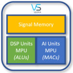
VSORA devised a compact and efficient approach combining advanced digital signal processing (DSP) with AI algorithmic acceleration, on the same silicon, exchanging data via on-chip large memory, setting a new standard for performance, power consumption, efficiency, area and cost. See figure 1.
Fundamentals of Autonomous Vehicles
To understand the issue, let’s consider a key AI application: autonomous vehicles. The brain or controller of a self-driving car operates on a three-stage loop: Perception, Planning, and Action. See figure 2.
Perception
In the Perception stage, the controller learns the environmental characteristics of the vehicle surroundings. This is accomplished by collecting a variety of data produced by a range of AV sensors, outside the scope of ordinary sensors monitoring the car’s status, such as oil and water temperature, oil and tire pressure, battery charge, light bulb functionality, and the like.
The AV sensors encompass a combination of different types of cameras, radars, lidars, ultrasonic devices, etc.. Actual type and quantity depend on vehicle manufacturers. For example, Tesla elected not to use lidar sensors.
The data generated by these sensors is processed via compute-intensive DSP algorithms to extract accurate and vital information to ensure safe AV driving.
The higher the level of autonomy of the vehicle, the more the vehicle relies on the accuracy and timeliness of what the sensors provide.
Autonomous Vehicle Sensors
AV sensors can be grouped in two broad classes: “cost-effective” and “high-performance.”
Both types of sensors capture data from the vehicle’s environment and elaborate it in-situ via pre-defined algorithmic processing before sending them to the controller. The difference is in the handling of pre-processed data.
In cost-effective sensors, pre-processed data is further run through local algorithms, for instance, tracking that generates lists of tracked objects dispatched upstream to the controller. For example, a sensor, be it radar, lidar or camera, may detect a series of objects in front of the car and then run them through a local image classification algorithm in an attempt to identify a pedestrian about to cross a road.
In high-performance sensors, the pre-processed data from all sensors is fed straight through to the controller where it is run through a series of algorithms. For example, fusing this data with data captured from other sensors for the same object, or clustering that combines multiple detections into bigger units, or distance transforms, or particle filter, typically some type of Kalman filter. While the data is unique to each sensor, it corresponds to objects that can be represented by vectors in the real world (x,y location, distance, direction of travel, speed, etc.). Once ensured that all the vectors from all sensors are aligned and use the same reference frame, each vector is positioned on an x-y grid in a map. The 2D map populated with the vectors encompass the vehicle environment and can be described using a 2D matrix. See figure 3.
The complex processing generates tracking information. To prevent false information, the controller may track many more objects than what is being presented, and through a decision process resolve to track-and-show the object or continue tracking the object or to delete it from further consideration. An example of the input information to the first stages could be the 3D lidar cloud and the 2D and/or 3D camera images.
The two types of sensors lead to significant differences in the system requirements.
The local algorithms in cost-effective sensors reduce the computing power of the controller and the data-transfer bandwidth of the communication with the controller. However, the advantages trade off accuracy because of imperfections in the sensors. In poor light conditions, or bad weather, sensors may generate incomplete and ambiguous data that may cause serious problems. Missing a pedestrian crossing a road in a blizzard because the camera failed to identify the pedestrian may have dramatic consequences.
In high-performance sensors, the amount of data traffic between sensors and control unit is significantly higher, demanding larger bandwidth and by far more computing power in the controller to combine and process data from several sensors in the time frame available. The upside is more accurate decisions since they are based on all sensor data.
The bottom line is that the Perception stage in the AV control unit is greatly dependent on powerful DSP, heavy data traffic and intense memory accesses.
Challenges
The IEEE article titled “Fusion of LiDAR and Camera Sensor Data for Environment Sensing in Driverless Vehicles“ states that “heterogeneous sensors simultaneously capture various physical attributes of the environment.” However, “these multimodal sensor data streams are different from each other in several ways, such as temporal and spatial resolution, data format, and geometric alignment. For the subsequent Perception algorithms to utilize the diversity offered by multimodal sensing, the data streams need to be spatially, geometrically and temporally aligned with each other.” See figure 4.
The requisites pose a series of challenges, such as, how to create a geometrical model to align the sensor outputs, how to process them to interpolate missing data with quantifiable uncertainty, how to fuse distance data; how to combine 3D point cloud from a Lidar with luminance data from a camera, and more.
To make an autonomous vehicle reliable, accurate and safe, it is imperative to solve the above challenges.
As discussed above, collective AV sensors data is typically combined into an occupancy map that stores information of relevant individual objects. Clustering identifies objects in an occupancy map, and the addition of distance transforms to clustering increases the accuracy of tracking and of the entire system. See figure 5.
When tracking objects, it is crucial to know where they are at any given time, and to predict where they may be in the near future. While implementing prediction is relatively simple, the problem explodes in complexity as the number of objects to be tracked increases. The issue gets aggravated when objects disappear and reappear for various reasons. For instance, when tracking two objects moving in different direction, and suddenly one object overlays and hides the other.
Distance transform improves algorithmic decisions by identifying distances between objects, and thereby helps overcome or reduce sensor induced errors and anomalies. Clustering also helps to reduce the decision trees. The probability to have an accurate information on an object increases substantially with 300 parallel pings on it vs. a single ping. The same also helps to deal with starting and ending tracking of a real or false object.
An adaptive particle filter, typically based on Kalman filter, may be used for tracking framework. For example, implementation of a recursive Bayesian estimation algorithm can handle non-linear and non-Gaussian state estimation problems.
As important, low latency in the communication between the Perception and the Decision stage is essential for accuracy and reliability. Just to exemplify, at a speed of 240 km/h, a vehicle would cover a distance of 67 meters in each second demanding system responses much faster than 1 second/iteration to avoid catastrophic outcomes.
The above considerations highlight the complexity of the task and the conspicuous computing power required to confront it. Only an advanced DSP implementation in an ad-hoc design architecture can solve the issues.
Planning / Decision
The Perception stage is followed by the Planning or Decision stage that establishes a collision-free and safe path to the vehicle destination. The objective is achieved by combining risk assessment or situation understanding with mission and route planning. These tasks require mustering vehicle dynamics, traffic rules, road boundaries and potential obstacles.
The traditional procedure for the Planning stage progresses through 4 steps. It starts with route planning that searches for the best route from the origin to the destination. Traffic information generated through C-V2X inputs may be included in this stage.
The second step determines the geometric trace the vehicle should drive on to reach the destination following set boundaries (road / lane) and traffic rules, whilst avoiding obstacles.
The third step deals with manoeuvre choice. Based on vehicle position and speed, manoeuvre comes up with the best vehicle actions to realize the specified path identified in step 2. As an example, best action among “turn right”, “go straight”, “change lane to the left”, etc.
Finally, the fourth step deals with trajectory planning, i.e., the vehicle’s actual transition from one state to the next in real-time. It involves vehicle constraints and navigation rules (lane/road boundaries, traffic rules, movement, …) while at the same time avoiding obstacles on the planned path (other vehicles, road conditions,…). Since trajectory planning is both time and velocity dependent, it can be regarded as the actual motion planning for the vehicle. During this time, the system evaluates errors between actual location and planned trajectory to revise the trajectory plan if needed.
The bottom line is that the planning stage in the AV control unit is greatly dependent on powerful AI processing and intense memory accesses.
Action: Execution/Control
The final stage in the autonomous vehicle controller is the Action stage. This stage implements the trajectory plan computed by the planning stage. For example, activating a turn-signal, moving to an exit lane, and turning off the present road. As the actions get executed, the environmental situation changes, forcing the entire process to re-start from the Perception stage.
VSORA
VSORA, a startup with decades of experience in creating DSP designs for the wireless and communication industry, conceived a re-programmable, scalable, software-driven multi-core DSP/AI solution that ensures a cost-effective development.
At a high level, the VSORA architecture is similar to the DSP architecture described in figure 6.
Called Matrix Processing Unit (MPU) for handling multi-dimensional matrices, the device can be configured with a variable number of cores. Each core is also configurable by defining a set of parameters. For DSP applications, the number of ALUs can be programmed in multiples of 8, up to 1,024 per core. For AI applications, the number of MACs can be programmed from 256 to 65,536 per core. The cores can further be programmed in terms of quantization, on-chip memory sizes, etc.
The architectures of the two types of MPU are similar but not identical.
VSORA: Combining Signal Processing and AI
As discussed above, the design of a controller managing autonomous vehicles relays heavily on a variety of algorithms for signal processing and for AI, both requiring high level of performance, while keeping power consumption and cost to the minimum. To compound the issue, these algorithms are going through continuous refining and updating making a solution casted in hardware unacceptable.
The VSORA solution is unique in that the same hardware can easily handle both the Perception and the Planning stages of the controller loop as discussed above.
Specifically, the Perception stage could be mapped on an optimized DSP MPU, and the Planning stage on a second MPU configured to accelerate AI algorithms. The two MPUs share an on-chip large memory, with the DSP MPU writing the results into the memory and the AI MPU reading those results out of the memory, in sequence, preventing memory conflicts. See figure 7.
The setup eliminates the performance bottleneck associated with external memories caused by restricted data-transfer bandwidth. It also reduces latency and power consumption by drastically shortening the data path to/from memory.
The actual implementation of the entire system fits in a small footprint, consumes low power, provides high performance, and is remarkably efficient.
The VSORA architecture is ideal to serve the AI/ADAS industry.
Conclusions
Early implementations of a VSORA system consisting of 512 ALUs and 16kMACs with 32MWord of memory, based on 7 nm process technology node, fitted in a silicon area of approximately 25 sqmm. Running at 2GHz, the ALU MPU executed about 1T MAC/second, and the AI MPU delivered a performance of 65 TOPs.
The results meet the challenges posed by today’s autonomous vehicle. The architecture is scalable to the extent that by doubling the area to 50 sqmm, it would be capable to handle the requirements for the next generations of autonomous vehicles.
Special thanks to co-author Jan Pantzar, VSORA Sales VP.