RVN! 26 Banner revised (800 x 100 px) (600 x 100 px)

Veriest Meetup Provides Insights on Safety, Deadlocks

Veriest Meetup Provides Insights on Safety, Deadlocks
by Bernard Murphy on 10-01-2020 at 6:00 am

Veriest Logo min

I wasn’t familiar with Veriest, I’m guessing you may not be either. They are a design and verification services company based in the Tel Aviv area (Israel). The CEO, Moshe Zalcberg, was earlier GM for Cadence in Israel. Echoes for me of the early days working with Ajoy Bose in Interra. Veriest have a big emphasis in verification, for example jump-starting formal verification at Valens and teaming with Nuvoton to accelerate tight dynamic verification schedules. A Veriest meetup highlighted another and delightfully free service – sharing verification know-how. They host meetup events for verification knowledge sharing, inviting experts from other companies to speak on an area of their expertise. I attended one of these events in September, in which Jyotika Athavale of Intel spoke on functional safety and Laurent Arditi of Arm spoke on using formal for deadlock detection.

Jyotika on soft error-rate modeling

Jyotika is a PE at Intel based in Chandler. She shared insight into soft error rate modeling from a perspective of neural nets. This is highly topical area; we know about functional safety in “standard” logic in an SoC, but AI accelerators are always treated as black boxes for safety. Which of course isn’t a long-term solution. She quoted an MIT paper in which an approaching large truck could be mis-identified as a bird, potentially leading to a fatal collision. That this is possible shouldn’t be a surprise. We’ve already seen many papers on how pixel-level hacking can completely change image identification. Soft errors can do the same thing. Jyotika’s talk was on modeling that soft error rate.

She observed that errors can occur in the image memory and in weights, even in computation. The consequences though, based on their empirical studies, are that fatal errors (crash/hang) are more likely than a silent data corruption (such as the bird versus truck example). Here I gather she is talking about NNs implemented on multicore processors. It would be interesting to know how this might apply to systolic array architectures. She also observed that the training phase is inherently error-tolerant since it is a slow iterative process, though I don’t think the same claim could be made for inference.

Laurent on improving deadlock detection, debug

Laurent is a Sr. PE at Arm in the Nice area in France, particularly expert in formal verification. His topic was on a refinement to deadlock hunting. This is a popular application for formal modeling where problems may be difficult to find in directed or random simulation. This is one of those formal topics that takes a while to wrap your head around, but I think I’ve got it.

First, the standard approach to checking for a deadlock in formal is a liveness assertion – checking that something good eventually happens, here say getting an ack following a req . The problem is that such assertions are based on something called Linear Time Logic (LTL). LTL checks along just one time-path. You may prove there’s no deadlock along that path (it escapes) or perhaps there only appears to be a deadlock along that path. In the second case, maybe you didn’t wait long enough. Or maybe it needed a nudge to get out of a local trap. You can add fairness constraints to fix either problem, but constraints can also introduce bugs. They can also expose real problems, a good thing, but this process is pretty hit and miss. The real problem is that you didn’t check exhaustively along all temporal paths. To do that you need to use Computational Tree Logic (CTL). Not a problem for the core engines but assertion languages such as SVA have no way to represent a CTL assertion.

CTL checks generated by Questa formal

Laurent used Mentor Questa Formal for verification. Given a standard (LTL) liveness assertion, this will automatically also generate and run a CTL check under the hood. Which bypasses the problem of not being able to write these checks. You get both checks, in Laurent’s terms a maybe-escapable deadlock check (the LTL version) and the definitely not escapable check (the CTL version). Between these you can figure out if you have a problem. Then you can decide if you want to add constraints or pass back to design as a real bug. He makes the point that getting to this conclusion is much easier when you have both LTL and CTL checks.

Good insights. To register for future Veriest events, and to access the presentation video and slides of this last event, click here.

Also Moshe’s opening comments to the event here

Also Read:

Online Verification Meet-up With Intel and Arm!

Python in Verification. Veriest MeetUp

5 Talks on RISC-V


Achieve Superior Energy Efficiency – Body Bias for FDSOI

Achieve Superior Energy Efficiency – Body Bias for FDSOI
by Mike Gianfagna on 09-30-2020 at 10:00 am

Achieve Superior Energy Efficiency – Body Bias for FDSOI

Silicon on insulator (SOI) technology has been around a very long time. I recall five-inch wafers full of SoS (silicon on sapphire) devices while working at the RCA Solid State Technology Center back in the dawn of time. Today, the concept of silicon on insulator is alive and well. Companies like GLOBALFOUNDRIES offer a special process twist, called fully depleted silicon on insulator, or FDSOI. This technology offers FInFET-like performance in a much simpler and more cost-effective process technology to achieve superior energy efficiency.

I got a chance to preview an excellent webinar on the topic of FDSOI and some additional techniques called body biasing to further enhance power performance. The webinar is presented by Philippe Flatresse, director of business development and marketing team at Dolphin Design. Philippe has very deep knowledge of the technology presented. While earning his PhD degree in Microelectronics from the Institut National Polytechnique de Grenoble Philippe developed the LETISOI SPICE model dedicated to SOI technologies at CEA LETI. He then joined STMicroelectronics Central R&D to deploy SOI digital design activity. After ST, he joined SOITEC as an expert for digital applications to participate in the worldwide promotion of SOI technologies. Philippe has a very strong command of FDSOI and its application.

The specific technique Philippe discusses in the webinar is adaptive body-biasing. Case studies are presented for the approach in the GLOBALFOUNDRIES 22FDX technology. Philippe begins with an overview of the ways body biasing has been deployed. Body bias is used to dynamically adjust the threshold voltage (Vt) of a CMOS transistor. The subject of the webinar is adaptive body bias (ABB), which compensates for temperature variations in the low Vdd range and aging variations in the normal to high Vdd range.

Philippe discussed the ABB IP design kit, which is a collaboration between Dolphin and GF. He then reviews the various versions of ABB IP that are available and what applications best fit their use. Example results are then presented for a ARM Cortex M4 design on GF22FDX technology. The results presented are quite compelling. The ABB IP portfolio from Dolphin is quite flexible. Several use cases are presented. How to select the appropriate ABB IP driver size is also covered, as is selection and placement of timing monitors and process corners and various sign-off schemes.

Detailed, actual silicon results are covered by Philippe. This section includes statistical results with ABB on and off to show the technology’s impact, which is significant. Philippe then summarizes the various approaches covered and their impact. Two comments here caught my eye.

  • Design an energy efficient power management system in weeks instead of months
  • Do more with less energy

Regarding doing more with less, more includes functionality, performance, battery life, designer productivity, differentiation, market coverage and predictability and SoCs. Less includes constraints, dynamic and leakage power, risks, complexity, re-spins and customer support. There is something for everyone. 

If you want high power efficiency but don’t want to pay for a FinFET technology, you need to attend this webinar. The webinar will be broadcast on Tuesday, October 6 at 10AM Pacific time. You can register for the webinar here. You can also learn more about Dolphin’s adaptive body bias IP portfolio here.  This technology truly lets you achieve superior energy efficiency.


The Car Data Monetization Muddle

The Car Data Monetization Muddle
by Roger C. Lanctot on 09-30-2020 at 6:00 am

The Car Data Monetization Muddle

Four years ago, this month, McKinsey published a report – “Monetizing Car Data” – which continues to simultaneously haunt and mock the automotive industry. The report claimed that by 2030 the so-called “car data market” would be worth as much as $750B.

SOURCE: McKinsey

This report spawned dozens of internal car data initiatives at car makers and fueled the dreams of startups while draining the pockets of investors. Four years later the industry is still coming to grips with the meaning of the report and its impact – including the realization that a lot of that “value” was derived from prosaic matters such as customer retention and cost avoidance.

That being said, the effort to extract value from vehicle data is a noble if somewhat quixotic cause. The proposition was brought home this week when General Motors announced that its Super Cruise semi-autonomous driving function will require a $25/month subscription (or a $15 add-on for an existing OnStar subscriber). If vehicle data is so valuable, why on earth is GM CHARGING customers for the privilege of connectivity?

This begs the question as to why ANY car company is charging a subscription beyond anything more nominal than Tesla Motors’ $10/month premium connectivity package. Is access to Super Cruise worth more to the customer than an annual subscription to Netflix or Amazon Prime…combined?

I was watching a recording of Rupert Mitchell, chief strategy officer for WM Motor Technology Group Company of China, presenting at MOVE America last week in which he noted the importance of vehicle connectivity. Mitchell cites a newer McKinsey study of vehicle owners in China 61% of whom said they would switch brands for better connectivity.

SOURCE: McKinsey, WM Motor

Mitchell illustrated the importance of connectivity by describing how he got rid of the three-year-old Lexus hybrid that he used to drive in Hong Kong because when he was crossing bridges, such as the two-year-old Stonecutter’s Bridge in Hong Kong the satnav in his car showed him driving over water.

Mitchell’s experience reminded me of the I-35 bridge collapse in Minneapolis in 2007, which multiple map providers at the time struggled to account for in their navigation systems. Thirteen years later, the auto industry has yet to solve the bridge out problem largely because map providers and car makers haven’t solved the twin connectivity and map updating problem.

As the industry shifts – more rapidly than many originally thought – to electrified powertrains and in-dash systems powered by Google, vehicle connectivity will become even more essential. Consumers may be willing to pay something for some portfolio of services, but car makers must be mindful of what is lost where and when customers choose not to pay and prefer to disconnect.

Mitchell highlighted, near the end of his talk, his company’s use of “data walls” to represent live vehicle data with analytics from the company’s connected fleet of vehicles travelling throughout China. The WM Motor data wall (illustrated above) is not unlike similar data walls visible in the headquarters of most auto makers across China.

As I have noted in the past, Chinese auto makers produce nearly one third of all automobiles on the planet. (Don’t worry, only a tiny fraction of these vehicles are actually exported.) In spite of the enormous number of vehicles China is pouring onto its roads, the companies making those vehicles are increasingly focused on keeping track of every one of those vehicles and monitoring their performance and status. This is especially important for cars with electrified powertrains.

When Toyota announced a deal nine years ago with Microsoft Azure to build a connected car eco-system, I imagined Toyota CEO Akio Toyoda overseeing a global connected car command center where Toyota vehicles the world over could be monitored. Needless to say this did not happen and has not happened. In fact, Toyota has shifted its towering and as-yet unrealized cloud car plans to Amazon Web Services.

GM, too, has made many proclamations regarding its connected cars, and, yet, GM insists on charging customers for connectivity which has translated into a massive population of GM vehicles with inactive or only partially functioning on-board modems. GM may have a data wall of its own – but many of the cars in its network are not reporting their data.

WM Motor is but one in a growing cadre of Chinese car makers that are redefining the car driving and owning experience with connectivity. An idea that was born in the “West” – of connecting cars – has been most aggressively embraced in the “East.” Mitchell captures the value proposition most powerfully when he notes near the end of his talk that the data wall provides “a better idea on a real-time basis of the residual value of all of our cars on the road today.” What is that worth? $25 a month??


SkillCAD Layout Automation Suite has Over 120 Commands Backed by 60 Customers

SkillCAD Layout Automation Suite has Over 120 Commands Backed by 60 Customers
by Tom Simon on 09-29-2020 at 10:00 am

SkillCAD Layout Automation Suite

Cadence Virtuoso is by far the most popular layout tool for IC design. This is especially true at advanced process nodes. In my opinion one of the key reasons for this is its built-in extension language, SKILL. SKILL is a powerful tool to add time saving and customized functionality to the Virtuoso layout editor. For analog and custom design the command features developed in SKILL can really enhance the layout editing experience.

There is a long history and even a precedent for including an extension language in layout editors. Calma’s GDSI and GDSII each had built in languages going back to the late 1970’s. Back then, as is still the case, parts of the vendor’s own product offering were developed in the editor’s extension language. However, customers widely use extension language development to add a competitive edge to their layout environment.

In the early days of layout editing software, chip companies themselves developed their own layout editors and other EDA software. As time went on this shifted to the point where chip companies pretty much all now buy commercial software instead of developing it on their own. The same, it seems, is the  case for SKILL code to enhance layout editing features. Many chip companies used internally developed customized SKILL code. However,  as each new process was adopted   it became cost prohibited to both develop and support these layout extensions written in SKILL. Chip companies then began to buy commercial software packages written in SKILL to enhance their flows. This  lead to significant cost savings as these tools  leverages the SKILL commands developed  and tested  in conjunctions with foundries and the top semiconductor customers around the world.  In a nutshell, that is the SkillCAD advantage.

SkillCad develops SKILL code to improve layout design efficiency based on their customers’ design requirements. Because they have a single focus, they can produce SKILL code that can make many of the design tasks required in analog, RF and custom design easy and fast for designers. Advanced node design often call for complex structures, such as shielding, twisted lines or matched wires to minimize signal integrity issues. At the same time, there are a myriad of design rules that have to be followed when creating custom layout. SkillCad’s products can create these complex constrained structures rapidly and easily while ensuring they are correct by design.

Their Layout Automation Suite (LAS) has over 120 commands that help with the following operations:

array manipulation, bus routing, calculation and measurement, connecting metal to devices, density checks, device placement, dummy fill, labels, layer handling, metal path and path segments, metal coloring, multi-part path and guard rings, nets, pins, shape handling, slotted metal, track routing, vias, and viewing.

One subset of their commands deals with managing the layout environment to make it easier to use. Setting layer viewing colors and visibility can be tiresome when done manually. SkillCad LAS offers a rich set of commands to control these and other settings.

The SkillCad LAS commands for bus routing, array handling and connecting metal to devices speed up what are usually repetitive and slow tasks. Even just turning a bus structure 90 degrees can become a complex error prone operation if done manually. SkillCad offers a comprehensive set of connectivity driven commands for manipulating buses and connecting to instance pins. There are specific features for inductor design. These include via fill operations, guard ring generation, smart shape editing functions, etc. Last but not least, several command groups address requirements for 20nm and below, such as dummy fill and density checks, routing tracks and color-aware routing. In all there are over 120 commands that have been developed over the last 12 years in close consultation with analog, custom and RF design teams at leading chip companies.

SkillCad has put together user guides  that shows tutorials and how to use videos for every command in LAS. It is clear from watching it that due to their large customer base and disciplined development that LAS is optimized to offer complex functionality with an easy to use interface. The commands appear to work seamlessly in the Virtuoso environment,   the videos shows the commands going through their paces. More information and the video can be found on the SkillCad website. www.skillcad.com

Also Read:

CEO Interview: Pengwei Qian of SkillCAD

Webinar: A Practical Approach to FinFET Layout Automation That Really Works

WEBINAR: SkillCAD now supports advanced nodes!


Siemens PAVE360 Stepping Up to Digital Twins

Siemens PAVE360 Stepping Up to Digital Twins
by Bernard Murphy on 09-29-2020 at 6:00 am

Siemens PAVE360

The idea of a digital twin is simple enough. You use a digital model of a car, aircraft, whatever to test design ideas and prove your design will be robust across a wide range of scenarios before you commit millions of dollars and lives to proving out the real thing. As Siemens have accomplished in their PAVE360 platform. There are a couple of challenges in building such a twin. One is how much effort you want to put in to faithfully model all aspects of the design. Bearing in mind that it’s already hard to model whatever you consider to be the most complex aspect of your design. Which leaves you to abstract other features with simple and less accurate approximations.

The second problem is calibrating your model to reality. Without that feedback to fine-tune the digital twin, predicted behaviors can be wildly wrong. What you think you proved in your model was safe behavior in fact is not at all safe.

Getting to scenario coverage

All of which is very relevant to modeling self-driving cars and advanced ADAS systems. The range of scenarios these have to cover is mind-boggling. RAND Corporation talk of cars needing to be trained over billions of miles of travel, equivalent to more than 100 years of driving. Which of course is impractical but also raises questions of how good that coverage really gives you. Was that really 100 years of widely varied experience or one year of experience repeated 100 times? Simulating a digital twin, carefully calibrated to a real car, is a much better approach. You can run an arbitrary number of experiments in parallel, and you can plan for comprehensive coverage, including dangerous scenarios you wouldn’t attempt in a real car.

Calibrating the model

That addresses the volume of testing and coverage questions, but what about calibration? For that you need an autonomous car, tricked out with all the sensors, actuators and software necessary to that purpose. VSI Labs has developed an autonomous Ford Fusion testbed with extensive capability. Ouster LIDAR, FLIR thermal imaging and OxTS inertial navigation. HERE HD maps, Dataspeed by-wire control (throttle, steering, brake), and NXP and Arm for localization, detection/recognition and planning. Nira Dynamics for road friction modeling and Aptiv for radar detection and tracking. Bolton and Menk for signal phase and timing and Leopard imaging cameras.

Siemens PAVE360

And finally, Siemens for digital twin modeling through their PAVE360 platform. Siemens and VSI can correlate instrumentation data from what they see in the real car with what they see in the digital twin. Providing the calibration they need to ensure the digital twin remains faithful over a subset of scenarios, while still allowing the twin to explore a much wider range of scenarios in a realistic time.

David Fritz (Sr Dir for autonomous and ADAS SoCs at Siemens PLM) told me about a demo they ran at CES which attracted a lot of attention. The twin was modeling an autonomous car, driving itself around a curve. At which point it detected a semi-truck stopped immediately ahead, calling for some fairly aggressive braking. It hit the brakes, but there was a water puddle on the left side of the road. Modeling the difference in friction between right and left and the weight distribution in the car, the car fishtailed.

Naturally at the same time another car came from behind, planning to drive past the first car (which should have turned safely out of the way). The cars collided. You can’t model that sort of scenario in an idealized digital twin. That takes comprehensive modeling, careful calibration. And the ability to model across scenarios you wouldn’t want to try in the real world.

You can learn more about the PAVE 360 platform HERE.

Also Read:

Verifying Warm Memory. Virtualizing to manage complexity

Trusted IoT Ecosystem for Security – Created by the GSA and Chaired by Mentor/Siemens

Emulation as a Service Benefits New AI Chip


Altair HPC Virtual Summit 2020 – The Latest in Enterprise Computing

Altair HPC Virtual Summit 2020 – The Latest in Enterprise Computing
by Mike Gianfagna on 09-28-2020 at 10:00 am

Altair HPC Virtual Summit 2020 – The Latest in Enterprise Computing

On September 9 and 10 Altair held their high-performance computing virtual summit. Altair is a company with a large footprint. In their own words, “Altair is a global technology company that provides software and cloud solutions in the areas of data analytics, product development, and high-performance computing (HPC).” Their virtual summit did not disappoint. It was well-run, professionally produced and delivered strong, relevant information across a broad range of topics. I will attempt to summarize the latest in enterprise computing according to Altair.

Day 1 of the event was a plenary session devoted to topics of general interest. After attending a few virtual events, there are typically several “rough spots” that need to be negotiated. One is production vs. spontaneity. Pre-recorded presentations are predictable and reliable. You typically don’t have words dropping out or pets walking across the frame. On the other hand, they lack the genuine, spontaneous and engaging quality of a live stream. I believe Altair struck a good balance here. Bill Nitzberg, CTO of Altair PBS Works, kicked things off with a live introduction. He provided the transitions between the pre-recorded sessions as well. He is an engaging and high-energy speaker, so this helped a lot.

After the first day of presentations, a live Q&A session was held with all speakers. This was a very engaging and enjoyable session.

So, what was discussed on day 1? It was quite a lineup:

  • Keynote Session: Exascale Computing Project, Michael Heroux – Exascale Computing Project
  • PBS Professional 2020.1 Intro, Bill Nitzberg – CTO, PBS Works, Altair (Bill had the interesting task of introducing himself)
  • Hierarchical Scheduling for High-throughput Computing Workloads, Jeremie Bourdoncle – Senior Director, Enterprise Computing Core Development, Altair
  • Cloud Bursting: State of the Arts GUIs for Seamless Scaling, Chris Townend – Director, Enterprise Computing, Altair, Ian Littlewood – Product Manager, Enterprise Computing Core Development, Altair
  • Budgeting, Allocation Management and Workload Simulation, Ian Littlewood – Product Manager, Enterprise Computing Core Development, Altair

On day 2 of the event, there were two parallel tracks. One focused on high-performance computing and the other on semiconductors. Given the typical background of the SemiWiki audience, I’ll focus a bit on the semiconductor track.

Stuart Taylor – Director, Enterprise Computing Core Development, Altair presented two topics:

  • Saving Serious Money with License-first Scheduling
  • Design Flow Mapping and Optimization: The Tool Every VLSI Team Needs

Andrea Casotto – Chief Scientist, Enterprise Computing Core Development, Altair also presented:

  • Bringing Cost as Close as Possible to Exact Demand with Rapid Scaling

Some of you may remember Andrea. He was the long-time president of Runtime Design Automation, which was acquired by Altair in 2017. Andrea presented an excellent talk on a very relevant topic for cloud computing, one that I’ve had some experience with. He began his presentation by saying, “If you’re going to buy resources from any cloud vendor WATCH YOUR MONEY.”

Andrea provided some examples of runaway spending on cloud resources. This is quite easy to do actually. The good and bad news about the cloud is that you can get any compute resource you ask for. Not only do you get it very quickly, but you have to pay for it as well…

Andrea began by advancing the concept of “cloud elasticity.” The technology from Altair that Andrea discussed is called Rapid Scaling. Here is an important quote:

Rapid Scaling Brings the Cost as Close as Possible to Demand

What followed was a compelling discussion about methods to “right size” compute resources for the workload. There are a lot of good ideas in this presentation, some are patented. If you want to achieve the most efficient and cost-effective use of the resources from your cloud vendor, I highly recommend you listen to Andrea’s presentation.

You can see all the presentations from the Altair HPC Virtual Summit 2020 here. Check it out and see the latest in enterprise computing according to Altair.

Also Read

High-throughput Workloads Get a Boost from Altair

Interview with Altair CTO Sam Mahalingam

Six Essential Steps For Optimizing EDA Productivity


Webinar: Static Verification for RISC-V Cores and SoCs

Webinar: Static Verification for RISC-V Cores and SoCs
by Daniel Nenni on 09-28-2020 at 6:00 am

Aldec RISC V Webinar SemiWiki 1

RISC-V has been trending ever since it landed on SemiWiki in 2016.  Even more so now that Arm is in flux with the Nvidia acquisition. Verification is a fast growing EDA challenge with the number of verification engineers steadily outpacing design, so this webinar is a best case scenario for SemiWiki traffic, absolutely.

Two things to note:

  • The presenter, Alexander Gnusin, is truly a verification expert. Before joining Aldec in 2017, Alex did ASIC design and verification at Freescale (Motorola), IBM, IDT, Nortel, and Ericsson plus a 3 year R&D stint with Synopsys.
  • Aldec is one of the strongest private EDA companies which offers you depth of experience (36 years) and approachablilty, both are key ingredients when facing leading edge verification challenges.

Here is the abstract and agenda. Register now and get the replay, no problem at all. I hope to see you there!

Abstract:
The entire processor industry is currently going through a paradigm shift – new generations of domain-specific proprietary processor cores based on the open-source RISC-V ISA are now being developed by various industry-leading semiconductor companies. Additionally, open-source RISC-V processor cores such as SweRV, Ibex and Pulp are now available, and they are actively being developed in various open-source Github communities.

Static verification or linting is a standard part of the tool flow for any processor-based designs to help engineers develop highly robust code in both IP and SoC levels. Static linting based on industry-best practice coding standards are critical in ensuring best-practice coding styles, efficient synthesis and timing closure, avoid simulation-to-synthesis mismatches, and proper usage of SystemVerilog constructs and data types. In this presentation, we will demonstrate how to statically verify RISC-V IP designs with the new ALINT-PRO RISC-V ruleset.

Agenda:

  • Current RISC-V design verification flow : the Overview
  • Advanced Linting with ALINT-PRO RISC-V Rules Plugin
    • ALINT-PRO Lintong for IP designs
    •  RISC-V Plugin overview
  • Running Advanced Linting on RISC-V designs:
    • Live demo of RISC-V cores linting
    • Issues & violations Analysis
  • Summary
  • QnA

Presenter Bio:
Alex accumulated 25 years of hands-on experience in various aspects of ASIC and FPGA design and verification. His employees list includes IBM, Nortel, Ericsson and Synopsys Inc. As Verification Prime for a multi-million gates project, he combined various verification methods – LINT, Formal Property checking, dynamic simulation and hardware-assisted acceleration to efficiently achieve design verification goals. He received his M.S. in Electronics from Technion, Israel Institute of Technology.

About ALINT-PRO
ALINT-PRO™ is a design verification solution for RTL code written in VHDL, Verilog and SystemVerilog, which is focused on verifying coding style and naming conventions, RTL and post-synthesis simulation mismatches, smooth and optimal synthesis, avoiding problems on further design stages, clocks and reset tree issues, CDC, DFT, and coding for portability and reuse. The solution performs static analysis based on RTL and SDC™ source files uncovering critical design issues early in the design cycle, which in turn reduces design signoff time dramatically.

About Aldec
Aldec Inc., headquartered in Henderson, Nevada, is an industry leader in Electronic Design Verification and offers a patented technology suite including: RTL Design, RTL Simulators, Hardware-Assisted Verification, SoC and ASIC Prototyping, Design Rule Checking, CDC Verification, IP Cores, Requirements Lifecycle Management, DO-254 Functional Verification and Military/Aerospace solutions. www.aldec.com


SMIC Cut off by US Government is Doomsday Scenario for US Chip Equipment Companies

SMIC Cut off by US Government is Doomsday Scenario for US Chip Equipment Companies
by Robert Maire on 09-27-2020 at 2:00 pm

US versus China Semiconductor

SMIC Cut Off = Worst case scenario
SMIC is on US gov “no fly” list for US Equipment Companies
Will likely lead to loss of all of China- 25% to 50% of revenues
Retaliation by China will worsen situation
SMIC cut off from US technology (Chip Equip)

It has been reported in the Wall St Journal and many news outlets that the US government sent out a “Dear John ” letter to US chip and equipment companies on Friday saying that SMIC is now on the “naughty list” and will need export licenses, which will be denied, to get US equipment.

U.S. Sets Export Controls on China’s Top Chip Maker

This essentially puts SMIC out of business…..

If Jinhua is any example, where all the US equipment companies got on the next plane out of Dodge leaving half installed equipment and open boxes, service, spare parts and all support is gone too.

The details of timing and impact are not yet out. Will equipment in the air get turned around? When does it take effect? What about foreign firms? Do US firms having manufacturing outside the US get a “loophole”? etc; etc; etc;

We told you so…

We have been talking about this issue for years , longer than anyone else. We have also been much more vocal about the risk.

Over two weeks ago we put out an article predicting exactly what has happened:

Could Chip Equip Co’s Lose China? Their Biggest Customer

While companies and analysts have played down or ignored this worst case scenario it is now reality that can’t be ignored.

It will likely extend to all of China…Not just SMIC

US Chip Equip Co’s will be placed on “Unreliable Entities ” list by Bejing

China has been threatening retaliation for the US cutting off Huawei. Before China even got the chance to respond the US government slapped them in the face with the SMIC cut off.

Bejing will likely put a lot of US companies on its “naughty list” but it may be more symbolic as it is “cutting off your nose to spite your face” type of behavior as China desperately needs that equipment to become free of the US.

China ready to put Apple, other U.S. companies in ‘unreliable entity list’: Global Times

There is a high likelihood that China’s response will up the game by a large measure and not just include the offending US chip equipment companies who won’t be allowed to ship chip equip to China but will also up the ante by adding giants that are big targets, such as Apple, intot he ever widening trade war.

ASML gets company

We had previously pointed out many times that it was greatly hypocritical for the US to ask the Dutch to stop ASML from exporting an EUV scanner without asking the same sacrifice of its own companies. Well ASML now has company in the “can’t ship to China ” club.

Our next question is what about Japanese companies especially Tokyo Electron? We can’t imagine the US will standby and watch them pick up all the lost US market share. The same goes for Korea and others. This will obviously escalate into a world trade war

Politics plays a big role

As we have previously pointed out politics plays a very big role as we are counting down to an election where being tough on China is a big talking point and most all US equipment companies are in blue states that effectively don’t exist and already are on a political “naughty list” as being part of the silicon valley opposition. This means that the potential financial ruin for chip equipment companies doesn’t much matter and certainly matters a lot less than soy bean farmers.

Other Chinese fabs will get on the list

SMIC was the obvious first and biggest target but its quite clear that what can be said about SMIC can be said about every other Chinese fab including the memory fabs.

To suggest that military applications don’t need memory is obviously a joke.

One of the big questions is foreign owned fabs located in China, such as Intel and Samsung etc? They will likely still get equipment but they are not leading edge nor critical to China getting technology.

Expansion plans in China will likely go on hold and expansion will slow or stop.

Semiconductors are a zero sum game-so who wins?

As demand for chips is a relative constant, they have to come from somewhere. If not SMIC and China then from who? Global Foundries is too far behind the leading edge to be real competition but could pick up some trailing edge business as they are not as far behind SMIC as they are behind TSMC.

TSMC will likely get the lions share of SMIC’s lost business and its trailing edge fabs may need expanding.

Even smaller companies like Tower-Jazz could see a pick up in business. Micron and Samsung could pick up memory business if China’s memory fabs get cut off but will likely also lose business after being placed on the unreliable entities list.

At the end of the day, chip equipment will get sold to someone else but clearly not as much as China was buying as China was on a catch up buying spree and spending more than needed for its current capacity.

Are the channels already stuffed?

We have been hearing for some time now that the Chinese are not stupid and have been on a buying spree for not just chips but also equipment in front of this embargo.

This clearly has played a part in some of the higher levels of business we have seen coming out of China.

This makes the fall in revenue even more precipitous as it is from an artificially high level to a near zero.

SMIC had been raising a lot of money to go on a spending spree, as we pointed out in our last note, and now much of that is going to go unspent.

Cold Turkey or an “organized wind down”?

One key issue which will determine the financial impact and wether equipment companies have actual losses (which hasn’t happened in a long time) will be if the impact is cold turkey or will take time to give them a chance to react.

The details are not out yet but we would vote that given the current political situation that the SMIC embargo will be more cold turkey, like Jinhua, than a slow wind down.

Obviously the September quarter is already in the bag but the December quarter could be very ugly. I think that most companies won’t be in the mood to give guidance in a few weeks as all bets may be off.

Much worse than Covid

The reality is that Covid while bad for the industry, was more of a temporary logistics problem that could easily be worked around. An embargo is much harder to get around. Much more important is the long term damage of trust between the US and China as China will avoid like the plague, any equipment made in the US.

Given that China was the fastest growing geography for every US equipment company and has grown to be everyone’s biggest revenue source, the impact will be huuugge.

The stocks

We have warned investors to stay out of the stocks as they had gotten way over priced and even with the recent pull back still had way to much risk.

All the equipment stocks will get whacked….there will not be much of any place to hide.

SMIC will get trashed. TSMC continues to win even more. Tower Jazz may be a good buy. Micron may be a neutral to a negative. Intel may get put on the naughty list but does have a facility n China.

Tokyo Electron may be a temporary bump up.

KLA and AMAT are most exposed while Lam is not far behind even though it is the memory “poster child”.

As always, the subsuppliers, ICHR, AEIS, MKSI, UCTT will get whacked more than their customers.

Materials suppliers remain a somewhat defensive play such as FORM, Cabot and Entegris. Photronics is a harder call given its large expansion into China which could be both a benefit and a risk.

Nova, being Israeli based, could see benefit by picking up share. VECO is less impacted as it has already lost virtually all of its China business.

Buckle up!….its going to get very, very ugly!


How to multiply currents: Inside a Counterfeit Analog Multiplier

How to multiply currents: Inside a Counterfeit Analog Multiplier
by Ken Shirriff on 09-27-2020 at 10:00 am

Inside a Counterfeit Analog Multiplier

A recent Twitter thread about a counterfeit analog multiplier chip attracted my attention since I’m interested in both counterfeit integrated circuits and how analog computers multiply. In the thread, John McMaster decapped a suspicious AD633 analog multiplier chip and found an entirely different Rockwell RC4200 die inside. Why would someone do this? Probably because the RC4200 (1978) currently sells for about 85 cents, while the more modern laser-trimmed1 AD633 (1989) sells for about $7.2

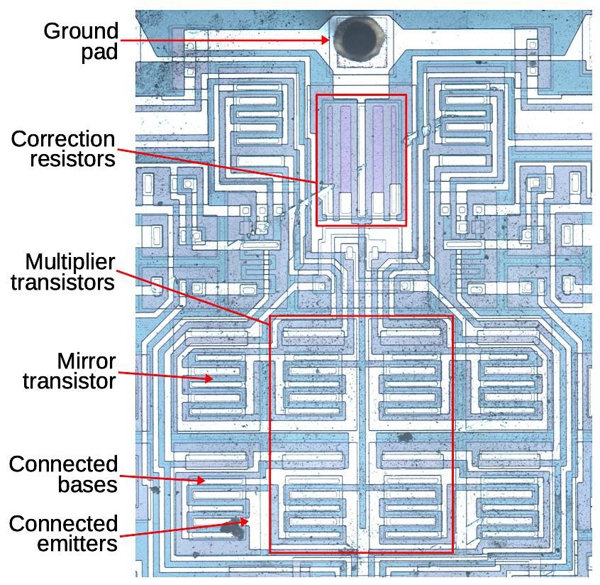
Die of the RC4200 analog multiplier with functional blocks labeled. Die photo courtesy of John McMaster.


Analog multiplication

Analog multiplication has many uses such as mixers, modulators, and phase detectors, but analog computers are how I encountered analog multiplication. A typical analog computer uses voltages to represent values and is wired up through a plugboard to solve a particular equation. Adding or subtracting two values is easy with an op amp, as is multiplying by a constant. Integration seems like it would be difficult, but it’s almost trivial with a capacitor; analog computers excelled at solving differential equations.

Multiplying two values, however, was surprisingly difficult; multiplication techniques were slow, inaccurate, noisy, or expensive. One accurate but slow multiplier used the Rube-Goldberg configuration of servo motors turning potentiometers.3 A 1969 multiplier circuit uses a light bulb and photocells. A fast and accurate approach was the “parabolic multiplier”, built from numerous expensive high-precision resistors.4 The approach I’ll discuss is to multiply by adding the logarithms and taking the exponential. Inconveniently, this approach magnifies even small differences between the transistors. It is also very sensitive to temperature. As a result, this approach was simple but inaccurate.

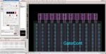
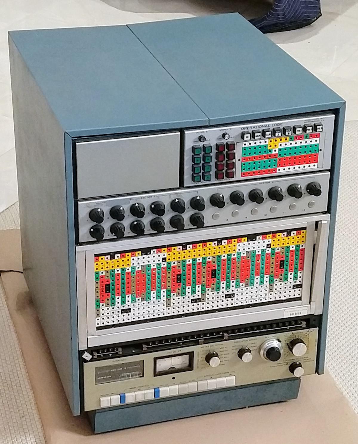
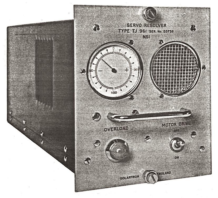
The Model 240 analog computer from Simulators, Inc. includes analog multipliers using the parabolic multiplier approach.


However, the development of analog integrated circuits created new opportunities for analog multiplication circuits. In particular, since the transistors in an integrated circuit were created together, they have nearly-identical properties. And the components on a tiny silicon die are all at nearly the same temperature.5

The first analog multiplier integrated circuit I could find is a television demodulator from 1967. The Gilbert cell technique was introduced by Barrie Gilbert in 1968 and is used in most analog multipliers today.6 The AD530 was introduced around 1970, and became an industry standard, but required external adjustments for accuracy. Laser-trimming the resistors inside the integrated circuit during manufacturing greatly improved the accuracy, an approach used in the AD633, the integrated circuit that was counterfeited.

Before explaining the circuitry of the RC4200 (the multiplier inside the counterfeit chip), I’ll discuss the components that it is constructed from, and how they appear in an integrated circuit. This will help you recognize these structures in the die photo.

Transistors

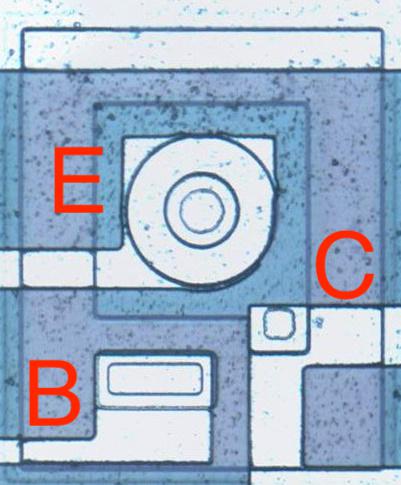
Transistors are the key components in a chip. The photo below shows an NPN transistor in the RC4200 as it appears on the chip. The different blue colors are regions of silicon that have been doped differently, forming N and P regions. The white lines are the metal layer of the chip on top of the silicon—these form the wires connecting to the emitter (E), base (B), and collector (C).

An NPN transistor on the RC4200 die. The emitter is embedded in the base, with the collector underneath.


You might expect PNP transistors to be similar to NPN transistors, just swapping the roles of N and P silicon. But for a variety of reasons, PNP transistors have an entirely different construction. They consist of a circular emitter (P), surrounded by a ring-shaped base (N), which is surrounded by the collector (P). This forms a P-N-P sandwich horizontally (laterally), unlike the vertical structure of the NPN transistors. The diagram below shows one of the PNP transistors in the RC4200.

A PNP transistor has a circular structure.


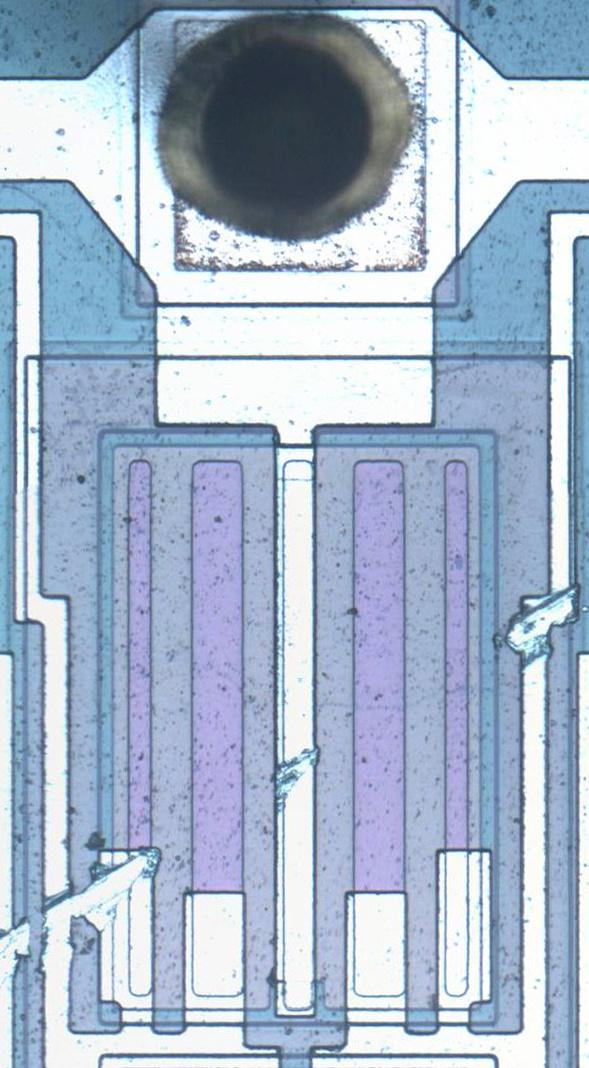
The input and output transistors in the RC4200 are larger than the other transistors and have a different structure to support higher currents. The photo below shows one of the output transistors. Note the multiple interdigitated “fingers” of the emitter and base.

A larger output transistor with parallel emitters and bases.


Capacitors

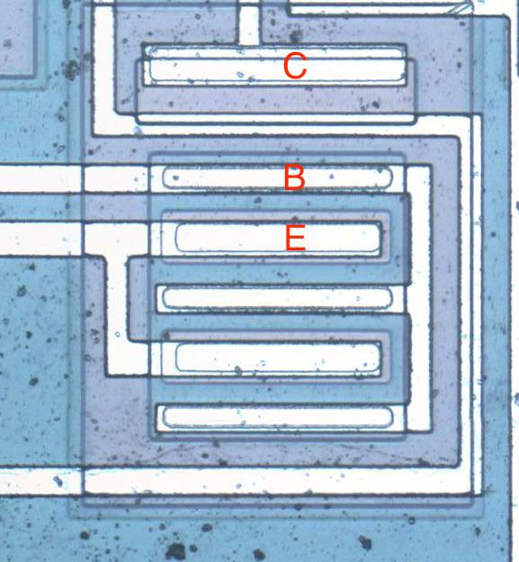
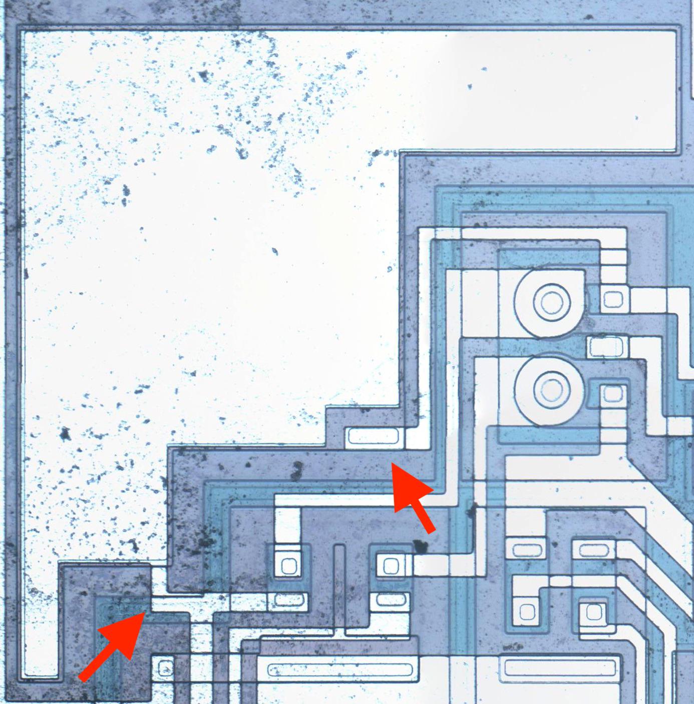
Capacitors are important in op amps to provide stability. A capacitor can be built in an integrated circuit as a large metal plate separated from the silicon by an insulating oxide layer. The main drawback of capacitors on ICs is they are physically very large. The 15pF capacitors in the RC4200 have a very small capacitance but take up a large fraction of the die area. In the photo below, the red arrows indicate the connection to the capacitor’s metal layer and to the capacitor’s underlying silicon layer.

The large metal area on the upper left is a capacitor.


Resistors

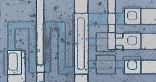
Resistors are a key component of analog chips. Unfortunately, resistors in ICs are very inaccurate; the resistances can vary by 50% from chip to chip. The photo below shows four resistors, formed using different techniques. The first resistor is the zig-zagging blue region on the left. It is formed from a strip of P silicon, with metal wiring (white) attached on the left and right. Its resistance is 3320 Ω. The resistor in the upper right is much shorter, so it is only 511Ω (long, narrow resistors have higher resistance than short, wide resistors). The remaining resistors are 20KΩ despite their small size because they are “pinch resistors”. In the pinch resistor, the square layer of brownish N silicon on top makes the conductive region much thinner (i.e. pinches it). This allows a much higher resistance for a given size. (Otherwise, a 20 KΩ resistor would be 6 times as long as the first resistor, taking up excessive space.) The tradeoff is the pinch resistor is much less accurate.

Four resistors, one on the left and three on the right.


Multiplying with logs and exponentials

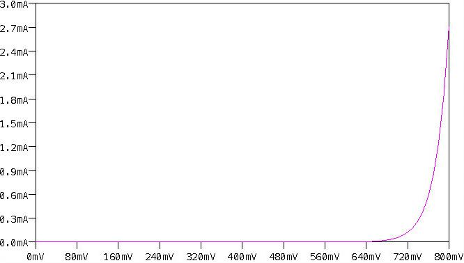
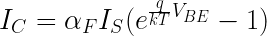
This integrated circuit multiplies using the log-antilog technique. The idea is that if you take the log of two numbers, add the logs together, and then take the antilog (i.e. exponential), you get the product of the two numbers. Conveniently, transistors have a logarithmic / exponential characteristic: the current through the transistor is an exponential of the voltage on the base. Specifically, if VBE is the voltage between the transistor’s base and emitter, the current through the collector (IC) is an exponential of that voltage, as shown in the graph below. The analog multiplier takes advantage of this property.

Ic vs Vbe curve for a transistor, showing the exponential relationship. Generated by LTspice.


The main complication with this approach is that the curve above is very sensitive to the temperature and to the manufacturing characteristics of the transistor. Because the curve is exponential, even a small shift in the curve will radically change the current. This was a serious difficulty when building a multiplier from discrete transistors, since the properties varied from transistor to transistor. To stabilize the temperature, some multipliers used a temperature-controlled oven. However, using an integrated circuit mostly solved these problems. The transistors in an integrated circuit are well-matched since they were built from the same piece of silicon under the same conditions. And the transistors in an integrated circuit die will be at almost the same temperature. Thus, integrated circuits made transistor-log circuits much more practical.

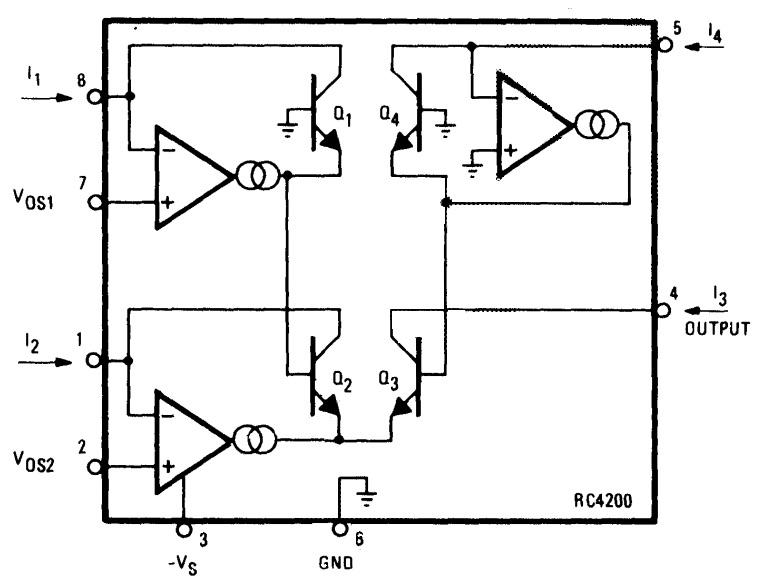
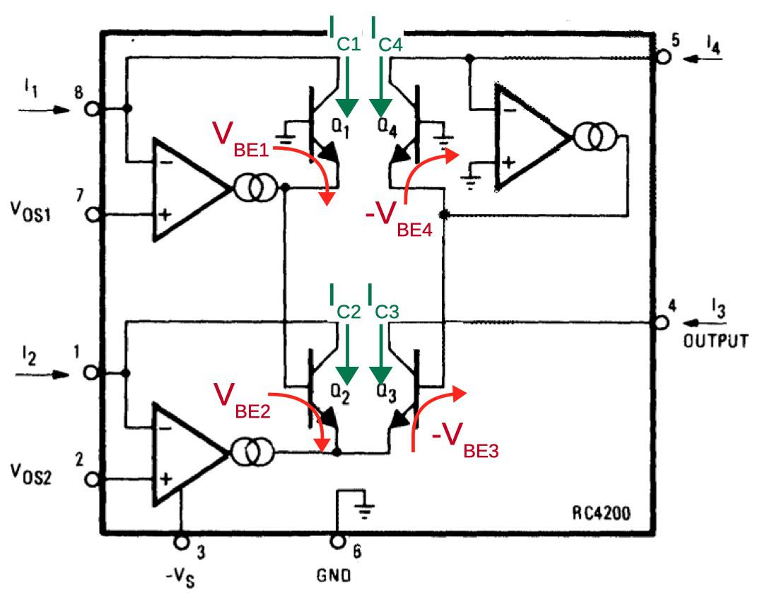
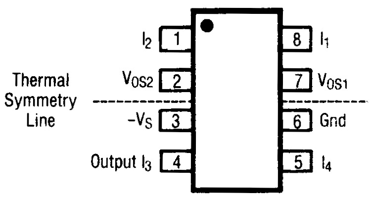
The diagram below shows the structure of the RC4200 multiplier chip. The user provides three current inputs (I1, I2, and I4) and the chip computes the output current I3, where I3 = I1×I2÷I4. (The use of current inputs and outputs is a bit inconvenient compared to other multipliers, such as the AD633, that use voltages.)

Structure of the RC4200 multiplier, from the datasheet. Note that the supply voltage (pin 3) is negative. VOS1 and VOS2 are offset adjustment pins to improve accuracy.


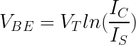
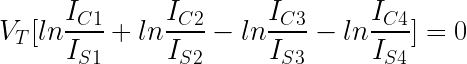
The four transistors in the middle of the diagram are the multiplier core, the key to the IC’s operation. The transistors are configured so their base-emitter voltages sum: VBE3 = VBE1+VBE2-VBE4. Because the transistor current is related exponentially to the voltage, the result is that I3 = I1×I2÷I4.

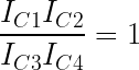
In more detail, first note that the voltages VBE1 through VBE4 control the collector currents IC1 through IC4 through the transistors (below). The op amps adjust the base-emitter voltages so the input currents match the transistor currents, i.e. I1 = IC1 and so forth. (This is accomplished by op amp feedback.) Now, if you go through the loop of base-emitter voltages starting at the base of Q1 and ending at the base of Q4 (red arrows), you find that VBE1+VBE2-VBE3-VBE4 = 0. (The voltages must sum to zero since you start at ground and end at ground.7) Now, because IC is related to exp(VBE), taking the exponential of the equation yields IC1×IC2÷IC3÷IC4 = 1. (Details in footnote8.)

Traveling around the loop indicated by the arrows, the voltages must sum to 0.


Next, I’ll explain how the VBE voltages are generated. Each current input has an op amp associated with it that produces the “correct” VBE voltage for the current using a feedback loop9 For example, suppose IC is too low so not all the input current flows through the transistor. The excess current will raise the voltage on the op amp’s negative input, causing it to reduce its output voltage and thus the transistor’s emitter voltage. This raises VBE (since the base will now be higher compared to the emitter), causing more collector current to flow through the transistor. Similarly, if too much current is flowing through the transistor, the op amp’s input will be pulled lower, reducing VBE. Thus, the feedback loop causes the op amp to find the exact VBE for the current input.10

Correcting for emitter resistance

The above circuit works reasonably well, but there’s a complication: the transistors have a small emitter resistance R. The voltage drop across this resistance will increase VBE by ICR, disturbing the nice exponential behavior. This creates a nonlinearity that reduces the accuracy of the result. The datasheet says that “Raytheon has developed a unique and proprietary means of inherently compensating for this undesired term.” They don’t explain this further, but by studying the die I have figured out how it works.

In the compensation circuit, each of the four multiplier transistors is paired with an identical “mirror” transistor with the corresponding emitters and corresponding bases connected, as shown below. These connections give the paired transistors the same base and emitter voltages, so they have the same collector currents. In other words, they form a current mirror. The mirrored currents are fed into special correction resistors that match the undesired emitter resistance, 0.1 Ω according to the datasheet.11 The voltage across the correction resistors will be the same as the excess voltage that needs to be compensated (since the resistance and current are the same). The final step is the correction resistors are connected to the base of the multiplication transistors, replacing the connection to ground. This will shrink VBE by the amount it was erroneously increased, fixing the computation.

The main multiplier consists of four transistors. Each transistor has a mirror transistor generating the same current, used to correct for emitter resistance.


Why are there two correction resistors? Recall that the multiplier has two transistors adding and two transistors subtracting (i.e. VBE1+VBE2-VBE3-VBE4 = 0). To handle this, the correction circuit is split in two. The left half sums IC1 and IC2 and applies this current to a correction resistor on the Q3/Q4 side, while the right half sums IC3 and IC4 and applies this to a correction resistor on the Q1/Q2 side. The addition and subtraction work out to yield the desired net correction.
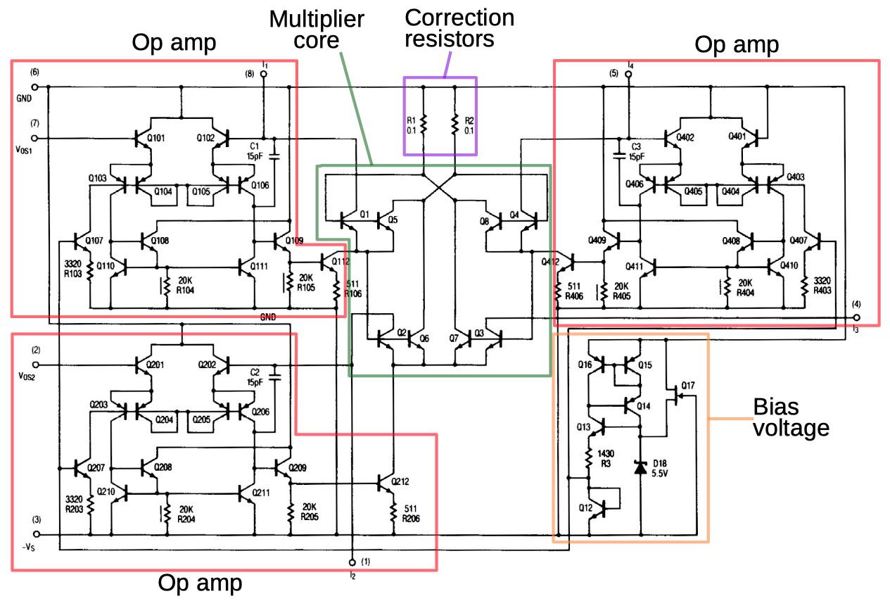
Schematic

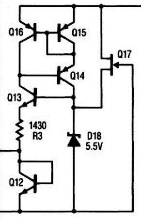
The schematic below shows the complete circuitry of the RC4200; I’ve highlighted the main functional blocks. (Inconveniently, I didn’t find this schematic until after I’d traced out the circuitry from the die photo.) The multiplier core and the correction resistors were discussed above The op amps circuits are fairly similar to the 741 op amp, which I’ve written about. They lack the output stage of typical op amps; the output transistor (Q112/Q212/Q412) corresponds to the intermediate gain state in a typical op amp. The bias circuit (orange, lower right) provides a fixed bias voltage for the op amps.12

Schematic from the datasheet, with main functional groups labeled.

Conclusion

Before integrated circuits, analog multiplication was difficult to implement. However, integrated circuits made it easy to create matched transistors, leading to fast, inexpensive analog multiplication integrated circuits. Unfortunately, analog multiplier integrated circuits were introduced just as analog computers were dying out, killed by inexpensive digital microprocessors, so analog computing missed most of the benefit of these chips.

While most analog multipliers use a circuit called the Gilbert cell, the Raytheon RC4200 analog multiplier uses a different technique to multiply and divide values represented by currents. Although, it includes a special error compensation circuit to improve its accuracy, it is obsolete compared to accurate, laser-trimmed multipliers. Now, counterfeiters re-label RC4200 chips and sell them as the more-expensive AD633 multiplier.

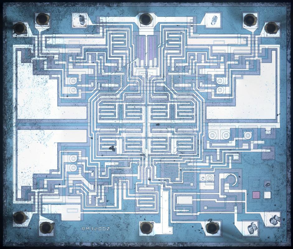
Die photo of the RC4200, courtesy of John McMaster.


I announce my latest blog posts on Twitter, so follow me at kenshirriff for updates. I also have an RSS feed. Thank you to John McMaster for the die photos used in this blog post; the photos are here.

Notes and references

  1. One reason that the AD633 multiplier is so expensive is that the resistors on the die are laser-trimmed resistors for accuracy. To get an accurate result, an analog multiplier requires exactly-tuned resistances. The older RC4200 requires adjustable external resistors, which is much less convenient. 
  2. I’m a bit puzzled by this counterfeit chip. Sometimes people will label a cheap op amp as an expensive op amp, as explained by Zeptobars. At first glance, that’s what’s going on here: a cheap multiplier repackaged as an expensive one. However, the two multipilers are so different that I can’t imagine one working at all in place of the other. Specifically, the AD633 takes differential voltage inputs and outputs two currents (a differential current), and it computes A×B+C. The RC4200, on the other hand, takes current inputs and outputs a single current, and it computes A×B÷C. 
  3. An example of a servo multiplier is the Solartron Servo Multiplier from the late 1950s. This 17-pound unit contained a potentiometer controlled by a servo motor, allowing it to multiply numbers represented by +/- 100 volts. It’s surprisingly fast considering its mechanical operation, responding in under 30 milliseconds. Power consumption was high: 70 watts, cooled by a fan. (In comparison, the RC4200 chip uses 40 milliwatts of power.)
    This photo shows the Solartron TJ961 Servo Resolver. This implements multiplication as well as sine/cosine computation. Photo from manual via Analog Museum.


  4. The 1969 analog computer I’m restoring uses a parabolic multiplier, a technique used for high-accuracy multiplication. The idea is that to compute A×B, you compute ((A+B)^2 – (A-B)^2)/4, which has the same value. That equation looks much more complex than the original product, but is easier to implement on an analog computer because op amps can perform the sums, subtraction, and division by four. Squaring is easier than multiplication because it is a function of a single variable, so it can be implemented by an “arbitrary function generator”.
    Parabolic multiplier circuit board from a Simulators, Inc. 2400 analog computer.


    The photo above shows a function board from an analog computer that computes the square, i.e. a parabola. The board approximates the function by multiple piecewise-linear segments, each defined by resistors. (Note the extremely accurate 0.01% resistors on the left.) The metal block in the center holds diodes, temperature-balanced by the metal. Each diode is biased to turn on at a particular voltage; the diodes act as switches, selecting the appropriate resistors for each linear segment. Note the large amount of precision hardware required for multiplication; a single product requires two of these parabolic function boards as well as multiple op amps. 

  5. To minimize the effect of temperature on the integrated circuit, the critical multiplier transistors are placed close together in the center of the chip. If there is a thermal gradient across the chip, this will minimize the temperature difference between the transistors. (Compared to putting the transistors in the corners, for instance.) To reduce temperature gradients even more, the datasheet specifies a “thermal symmetry line”. Putting a temperature source on this line ensures that the hotter transistors will tend to cancel each other out.
    The datasheet shows the IC’s thermal symmetry line.


  6. Barrie Gilbert, inventor of the Gilbert cell, has a video explaining translinear circuit, circuits based on the exponential current-voltage relationship of a bipolar transistor. This video explains translinear analog multipliers in detail, discussing two approaches> The first approach, used by the RC4200, is the “log-antilog” approach, where op-amps force and sense the collector currents. The second, used in the AD633 and many other multipliers, is the “integrated” approach, built from voltage-to-current conversion, a differential current-mode core, and current-to-voltage conversion. 
  7. I should mention that the chip uses a -15 V supply, so ground is the highest voltage and the other internal voltages are all negative. Just a warning since this makes things confusing and backward compared to circuits where ground is the low voltage. 
  8. The relationship between the base voltage and the collector current is given by the Ebers-Moll model. This equation (below) is filled with interesting constants: α: a gain factor (almost 1), k: the Boltzmann constant, IS: the saturation current (extremely small, order of 10-15 A), T: the absolute temperature, q: the charge on the electron. (The temperature in the exponential term reflects the importance of temperature stability for the multiplier.)


    Substituting the thermal voltage VT (about 26 mV) for kT/q, making some minor approximations, and taking the log yields:


    Substituting that into the multiplier’s VBE loop equation yields


    Taking the exponential and assuming the transistors all have the same temperature and saturation current yields the desired equation relating the four currents:


    This equation shows how the four currents are related by multiplication and division. See the datasheet for more details. 

  9. In a sense, the op amps compute the inverse of the transistor’s exponential function. The transistor takes VBE as an input and produces the exponential current as an output. However, we have the current as the input and want the logarithmic voltage as the output. By using the op amp with a function in its feedback loop, we can find the inverse of a function, in this case giving us the logarithm. That is, the op amp will converge on the output X where f(X) equals the input, i.e. X = f-1</sup(input). The same technique can be used to generate a square root from a multiplier chip: use the multiplier to square its input, and then use an op amp to compute the inverse function, i.e. the square root. 
  10. You might wonder why the op amp finds the “correct” value and doesn’t overshoot and oscillate. Handwaving away all the theory, the idea is that the capacitor on the op amp input stabilizes it and prevents oscillation. Even so, the datasheet warns that the circuits become unstable as the input currents approach 0. This corresponds to dividing by zero, so it’s not surprising that the circuitry doesn’t handle it well. Mathematically, the op amp is trying to find ln(0), which isn’t going to work. If you want to multiply by zero or negative values, the datasheet describes how the inputs can be biased with resistors to keep the inputs positive but still get the correct answer. 
  11. The two resistors below are used for the emitter correction; they have unusual construction and a very small resistance, 0.1 Ω. Each resistor consists of the two vertical stripes, connected together at the bottom; the vertical region in the center is connected to the ground pin, forming the other side of each resistor. These resistors improve the accuracy of the product by correcting for the emitter resistances. Based on their purple color, which doesn’t appear elsewhere on the die, they appear to be specially doped. The metal contacts at the bottom cover part of the resistor; I believe that by adjusting the size of the metal contacts, the resistor values can be tuned. I believe that the thick and thin regions allow for coarse and fine tuning.
    Precise small-valued resistors provide a correction factor.


  12. The bias voltage circuit generates a stable voltage of one diode drop (about 800 mV) from Q4’s collector; this voltage biases the op amps. The tricky part is how to keep the power supply voltage from influencing this voltage or the Zener voltage.
    The bias generation circuit, from the datasheet.


    The idea is that the Zener diode puts 5.5 volts on the base of Q13. The voltage across R3 will be two diode drops lower (2.8 V) due to Q13 and Q12. This yields a fixed current of 2.8 V / 1430 Ω = 2 mA through Q4, resulting in a stable voltage drop across Q12 and a stable output. But a Zener’s voltage fluctuates a bit with current, so the clever part is how the Zener’s current is kept stable. Transistors Q14, Q15, and Q16 form a current mirror, so the current through the Zener will match the current through the resistor, which is 2 mA. Thus, the Zener voltage keeps the resistor current and output voltage stable, while the resistor current keeps the Zener stable. The final piece of the puzzle is the FET Q17, which provides a tiny current through the Zener to start the feedback cycle. 


Innovating to Survive

Innovating to Survive
by Vivek Wadhwa on 09-27-2020 at 8:00 am

Innovating to Survive

The global COVID-19 pandemic has almost shut down entire industries, forcing companies of all sizes to adapt and evolve. It has also done incredible things for a pivot to innovation.

Safety has had to come first. And for many, that meant changing how they worked, using technology to power a shift to remote work and servicing of customers. For some, like retailers, restaurants and manufacturers, it meant shutting down key services or production lines and pivoting to new offerings or entering new markets just to survive and stay relevant. Others, rather than just close doors, have repurposed their assets to contribute to the collective effort to fight the crises.

When commercial flights were shut down, airlines like Virgin Atlantic, Lufthansa, and American Airlines switched to cargo-only flights. In the UK, healthy fast-food chain Leon announced it was turning its 65 restaurants into shops, selling meals via both click-and-collect and delivery. Hotels started offering day rates for remote workers. And multiple manufacturers, like Scottish craft beer specialists BrewDog, converted their plants to produce hand sanitiser.

What does it take to shift this fast successfully? And is this kind of progress sustainable?

The reality is that it is not essential that we be thrown into crisis before this kind of change can take place.

With the enforced change in human movement and behaviour came a change in customer demand. Businesses had to think and act fast to repurpose assets, talent, resources, distribution channels, offerings. Minus the crisis, it’s what successful businesses do every day.

SpaceX’s giant step

On 11 April 2019 – before we knew what 2020 would bring – a Falcon Heavy rocket was launched Cape Canaveral, Florida, making history. It was the first in a new generation of space exploration: a rocket that would not only be able to pilot its way through space, but be able to navigate and return to Earth for re-use, radically reducing the cost of space travel.

To achieve this, SpaceX combined radical and creative funding systems, brilliant talent, and perhaps most importantly, vision. But the question at the heart of this isn’t – ‘how did SpaceX achieve this’; the question is why the incumbents didn’t? How has innovation and creativity become so stifled in large, established organisations that it takes a new kid on the block to go, quite literally, where no-one has gone before?

It’s about culture, leadership, and some very practical steps that enable businesses to be their own catalysts for change, rather than relying on a crisis to spark exponential change.

The DNA of organisations that thrive through change

From Incremental to Exponential, a book I have co-authored with Ismail Amla, looks at what it takes to drive exponential change in an enterprise. In it, we examine five common components that make up the DNA of organisations that thrive through change.

  • Firstly, speed. Leading companies just operate faster – from reviewing strategies to allocating resources. McKinsey research indicates that these companies relocate talent and capital four times more quickly than their less nimble peers.
  • Secondly, being ready to invent. While business need to maintain the profitable elements of what they do, operating at business as usual is dangerous. Leading businesses are investing as much in upgrading the core as they are on innovation.
  • Thirdly, being all-in. These companies aren’t just making decisions faster, the decisions themselves are bolder, braver and further outside of the box.
  • Fourthly, making data-driven decisions. Data is providing the fuel to power better and faster decision making. High-performing organisations are three-times more likely to say that data and analytics initiatives contribute at least 20 percent to EBIT. Which is profound.
  • And finally, following the customer. Top companies that sustain a comprehensive focus on the customer (in addition to operational improvements) have been shown to reap economic gains ranging from 20 to 50 percent of the cost base.

You’ll find a wealth of insight on what it takes for large companies to see the future and rethink innovation in From Incremental to Exponential, released in the US on October 6th.

Also, Ismail and I will be doing a series of podcasts on LinkedIn to discuss what it takes for legacy companies to reinvent themselves under the “Innovating to Survive” theme. I hope you will join us for these!