RVN! 26 Banner revised (800 x 100 px) (600 x 100 px)

Pitching Without a Net. Look Ma, No Slides!

Pitching Without a Net. Look Ma, No Slides!
by Bernard Murphy on 02-01-2021 at 6:00 am

Book Cover min

It’s a given in the business world that whenever you need to communicate to a group you need a slide deck. Yet we vigorously agree that most pitches are miserably bad, for all the usual reasons. All about the presenter’s product, not audience needs. A firehose of technical detail designed to drown any possible objection. A script to hide behind so the presenter won’t forget any points they want to make, and a convenient shield against anything the audience might have to say. Take a risk – consider pitching without a net.

When slides are a bad idea

We all nod, recognizing well these sins in others. Then we race off to commit the very same mistakes in our own pitches. Evidently knowing what not to do is not enough. Sometimes we need to reset, to ask what our audience wants from this interaction. Sometimes they want data, and a pitch may be as good a way as any to deliver that information.  Sometimes slides aren’t the right answer.

When your audience wants a discussion about their needs, especially if you’ve not been delivering to those needs, then slides are like a red rag to a bull. Whatever spin you put on them, slides say “I know how to fix the mess I made. You should listen attentively because I’m going to explain.” The worst possible place to rebuild a damaged relationship is to walk through a tedious exposition of your solution to a problem that, based on the evidence, you clearly don’t understand.

Ditching the pitch

I have to admit that I’ve messed up – many times. I’ve had to face angry customers, rebuild confidence that we were still the right choice. Like most of us, I’ve always prepared very carefully, slide deck at the ready, knowing that in some way I would have to explain our under-performance and our suggestions for climbing back out of the hole.

The real challenge is in knowing how to use that information in the meeting. Marching through the slides would be suicidal, see above. A more rational approach would be to have a discussion, let your customer vent, figure out their most pressing concerns and show a slide or two that might be relevant. Or maybe show a scaled back version of the pitch, trimmed to address your now improved understanding. Sometimes that does the trick. But I have also tried a different approach which can work even better, if you have the stomach for it. I give my pitch without slides.

It’s easier than you think

Two points here. First, I imagine you recoiled in horror at the thought of losing your precious slides, your safety net. Without that net you’ll surely fail. But as we constantly remind our customers, we shouldn’t let fear of failure outweigh the upside. And I’m not suggesting you shouldn’t build slides – only that maybe you shouldn’t present them.

Second, this doesn’t take a superhuman feat of memory. When I pitch in this way, I remember the main flow and some features from my slides. But I haven’t memorized them, and I don’t recite a mental walk-through. Instead, I tell a story of how we’ve been working to meet this valued customer’s needs, weaving in key points I remember from my deck.

What’s the upside? Without slides, the audience can’t read ahead. They have to listen to you. They have no time to misinterpret what you’re about to say or trip you up on ambiguities. You’re looking at them, so you see body language. The format is inherently interactive. If someone has a question, you can deal with it quickly. That builds trust – you’re paying attention to their feedback, you’re tracking what they care about, not what you care about. At the end of one memorable talk I gave, my initially hostile audience were thanking me for a great discussion. That’s an outcome that might be worth the risk.

Want to know more? I tell that story in The Tell-Tale Entrepreneur, along with several other stories on the power of storytelling in business settings.


Examining a technology sample kit: IBM components from 1948 to 1986

Examining a technology sample kit: IBM components from 1948 to 1986
by Ken Shirriff on 01-31-2021 at 10:00 am

box opened w700

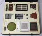
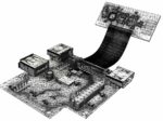
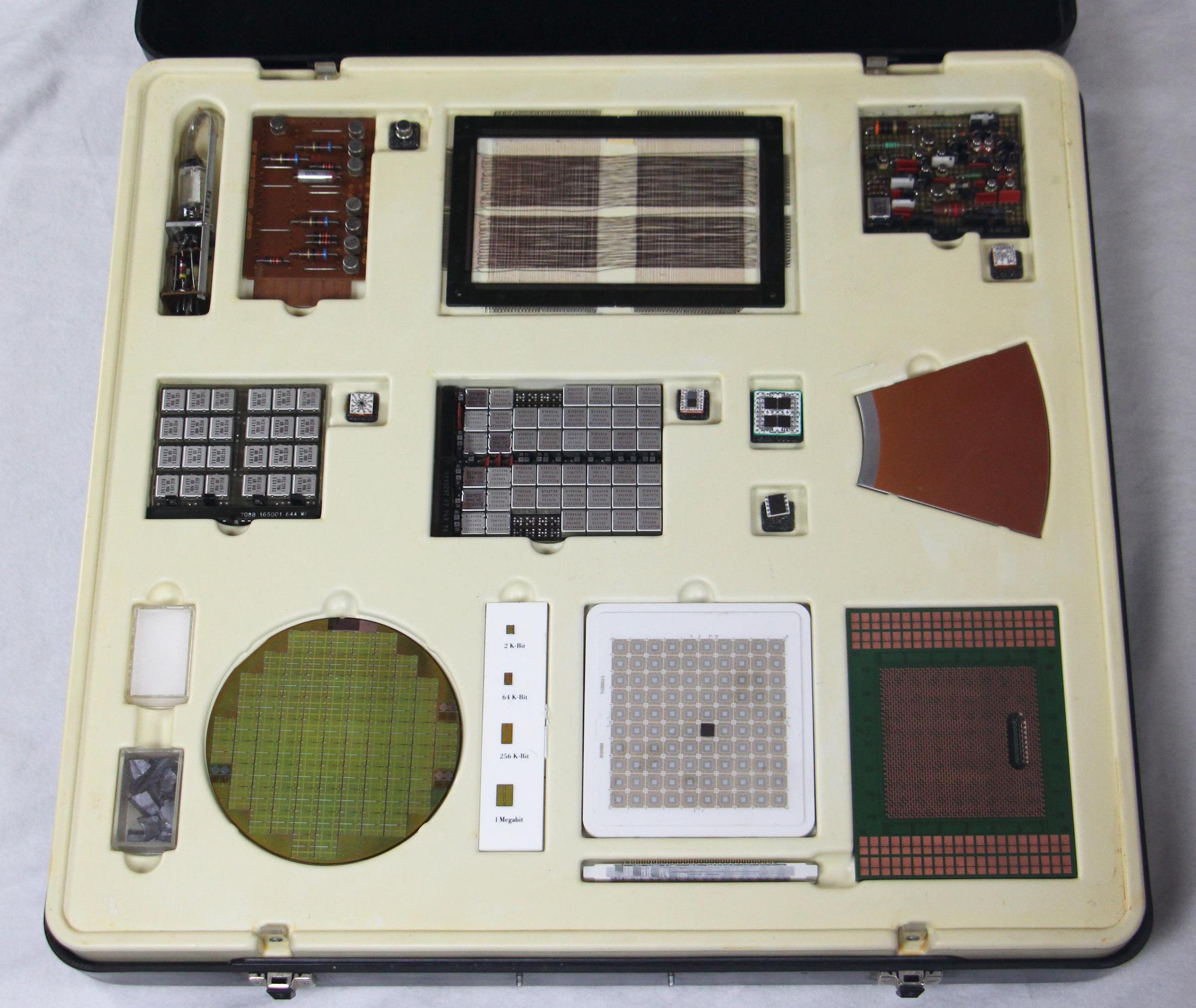
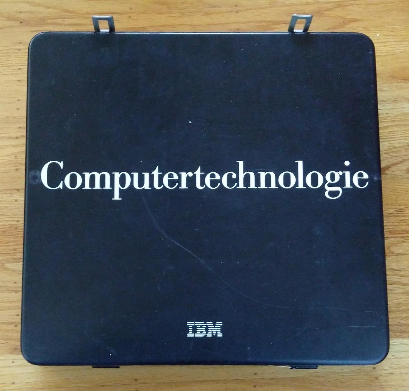
I recently received a vintage display box used by IBM to illustrate the progress of computer technology. This display case, created by IBM Germany1 in 1986 included technologies ranging from vacuum tubes and magnetic core memory to IBM’s latest (at the time) memory chips and processor modules. In this blog post, I describe these items in detail and how they fit into IBM’s history.

An IBM display box, showing components and board from different generations of computing. Click this (or any other photo) for a larger image.

First-generation computing: tube module

IBM is older than you might expect. It was founded (under the name CTR) in 1911 and produced punched card equipment for data processing, among other things. By the 1930s, IBM was producing complex electromechanical accounting machines for data processing, controlled by plugboards and relays.

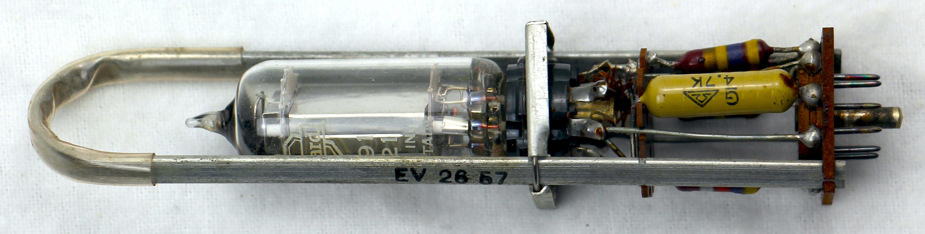
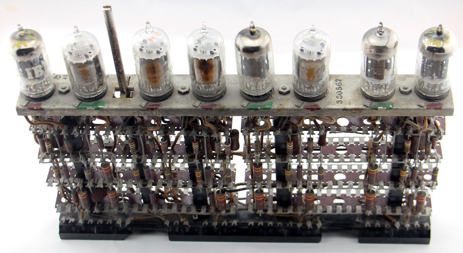
The so-called first generation of electronic computers started around 1946 with the use of vacuum tubes, which were orders of magnitude faster than electromechanical systems. Appropriately, the first artifact in the box is an IBM pluggable tube module. The pluggable module combined a vacuum tube along with its associated resistors and capacitors. These modules could be tested before being assembled into the system, and also replaced in the field by service engineers. Pluggable modules were also innovative because they packed the electronics efficiently into three-dimensional space, compared to mounting tubes on a flat chassis.

Tube module from an IBM 604 Electronic Calculating Punch.


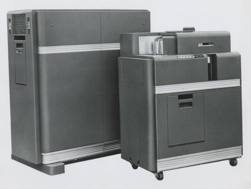
The pluggable tube module is from an IBM 604 Electronic Calculating Punch (1948). This large machine was not quite a computer, but it could add, subtract, multiply, and divide. It read 100 punch cards per minute, performed operations, and then punched the results onto new punch cards. It was programmed through a plugboard and could perform up to 60 operations per card. The IBM 604 was a popular product, with over 5600 produced. A typical application was payroll, where the 604 could compute various tax rates through multiplication.

The IBM 604 Electronic Calculating Punch behind a Type 521 Card Reader/Punch. Photo from IBM.


The 604 used many different types of tube modules. A typical module implemented an inverter, which could be used in an OR or AND gate.2 The tube module in the display box, however, is a thyratron driver, type MS-7A. The thyratron tube isn’t exactly a vacuum tube since it is filled with xenon. This tube acts as a high-current switch; when activated, the xenon ionizes and passes the current. In the 604, thyratron tubes were used to drive relay coils or magnet coils in the card punch.3

A thyratron tube, type 2D21. This tube is from the pluggable module in the box.


Although the 604 wasn’t quite a computer, IBM went on to build various vacuum-tube computers in the 1950s. These machines used larger pluggable tube modules that each held 8 tubes.4 The box didn’t include one of these modules—probably due to their size—but I’ve included a photo below because of their historical importance.

A key-debouncing module from an IBM 705. Details here.


Second generation: transistors and SMS (Standard Modular System) card

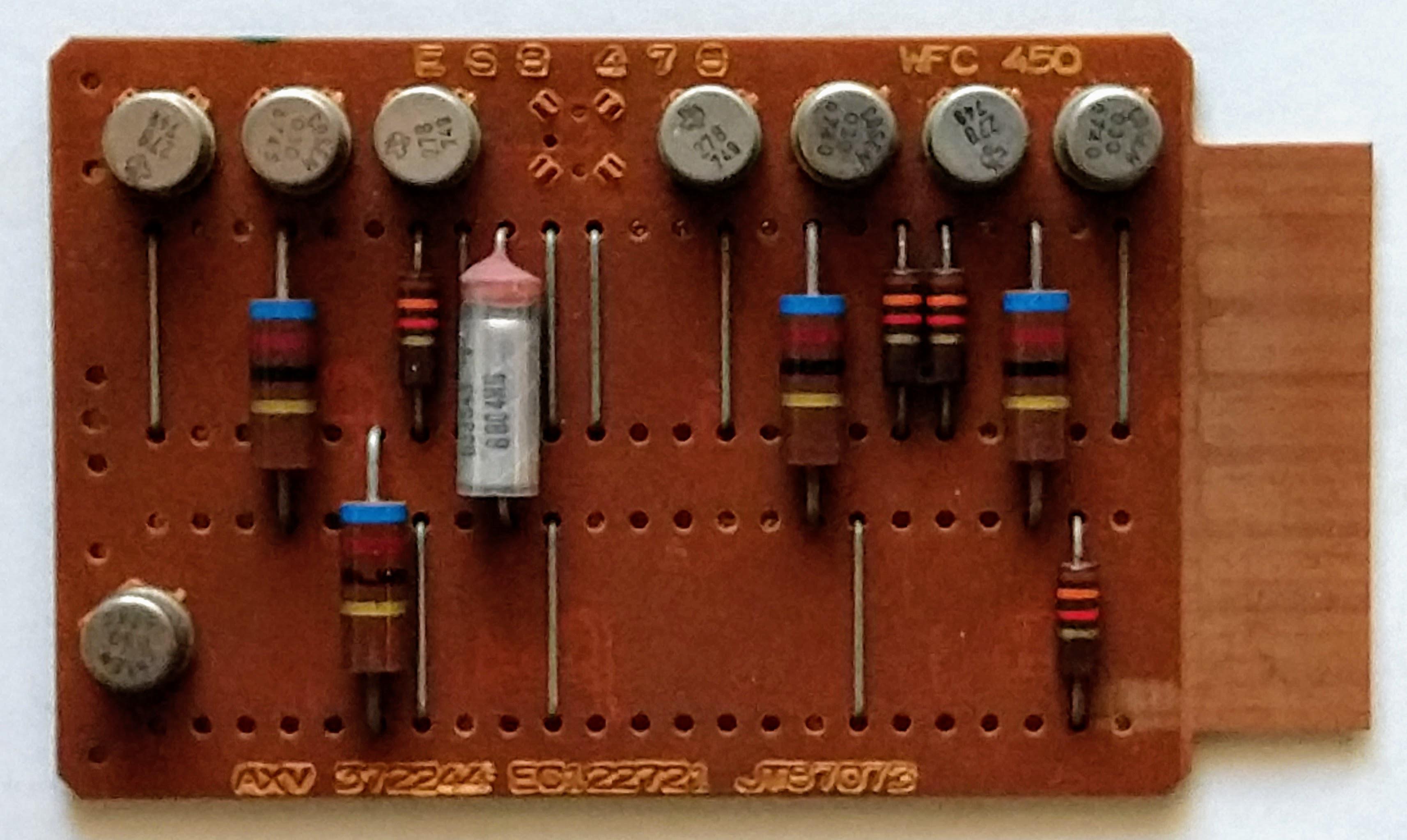
With the development of transistors in the 1950s, computers moved into the second generation, replacing vacuum tubes with smaller and more reliable transistors. IBM based its transistorized computers on pluggable cards called Standard Modular System (SMS) cards. These cards were the building block of IBM’s transistorized computers including the compact IBM 1401 (1959), and the larger 7000-series mainframe systems. A computer used thousands of SMS cards, manufactured in large numbers by automated machines.

The photo below shows the SMS card from the box.5 The card is a printed circuit board, about the size of a playing card, with components and jumpers on one side and wiring on the back. A typical SMS card had a few transistors and implemented a simple function such as a gate. The cards used germanium transistors in metal cans as silicon transistors weren’t yet popular. I’ve written about SMS cards before if you want more details.

The SMS card in the technology box, type AXV.

Third generation: SLT (Solid Logic Technology)

In 1964, IBM introduced the System/360 line of mainframe computers. The revolutionary idea behind System/360 was to use a single architecture for the full circle (360°) of applications: from business to scientific computing, and from low-end to high-end systems. (Prior to System/360, different models of computers had completely different architectures and instruction sets, so each system required its own software.) The System/360 line was highly successful and cemented IBM’s leadership in mainframe computers for many years.

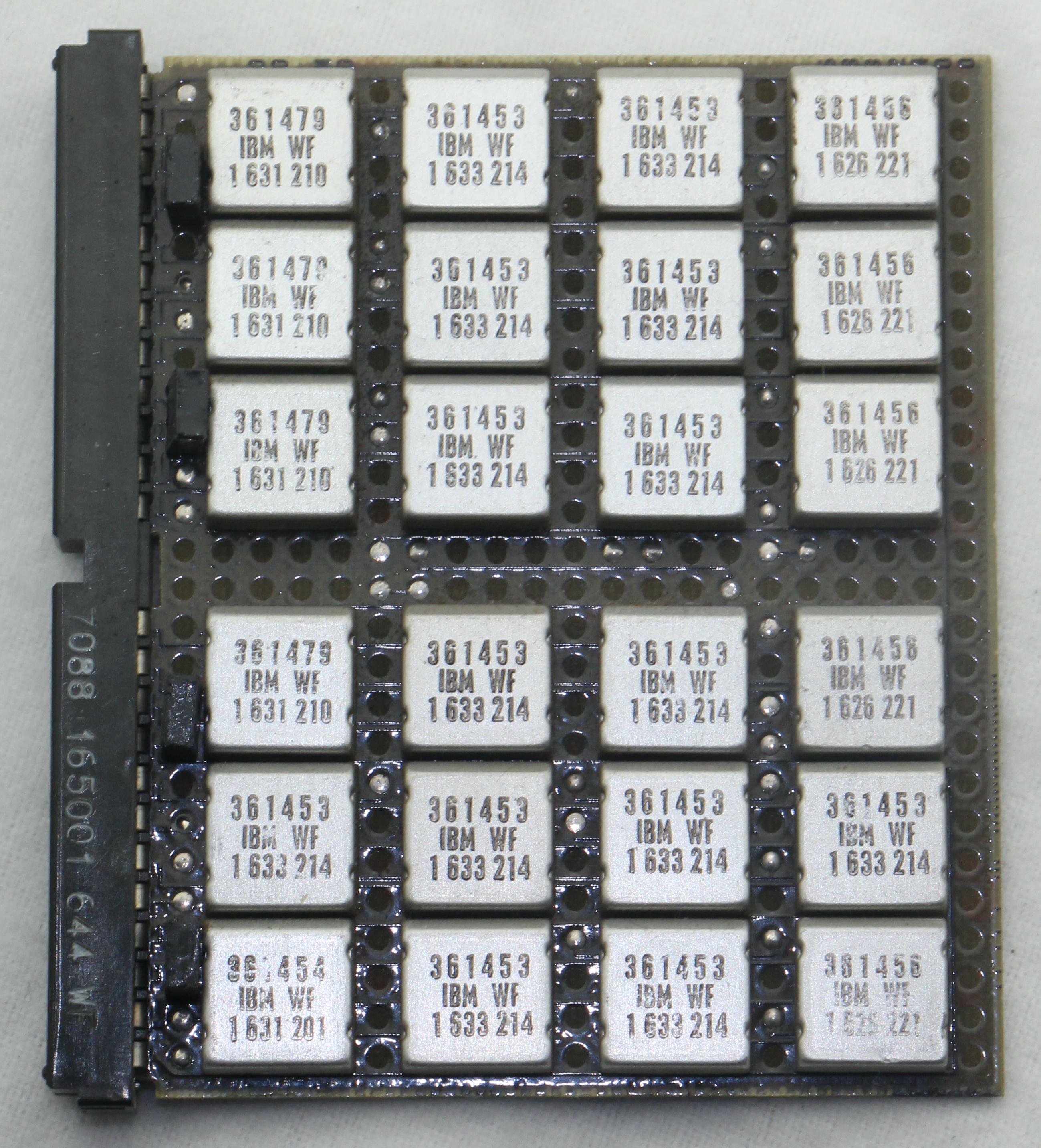
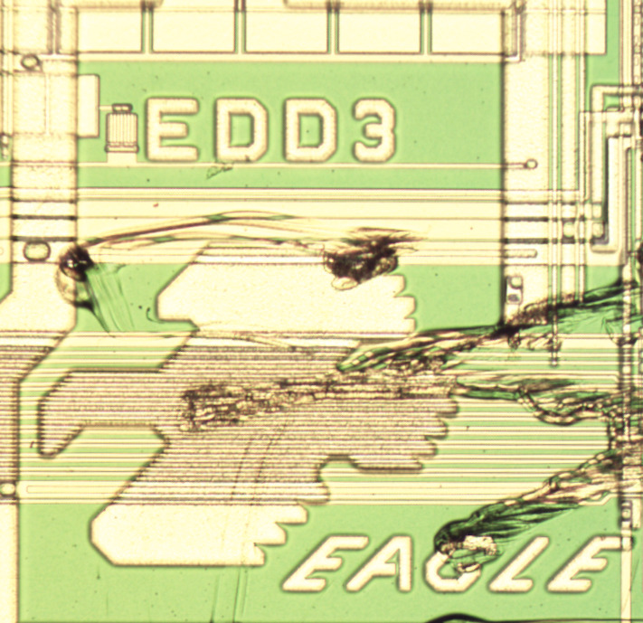
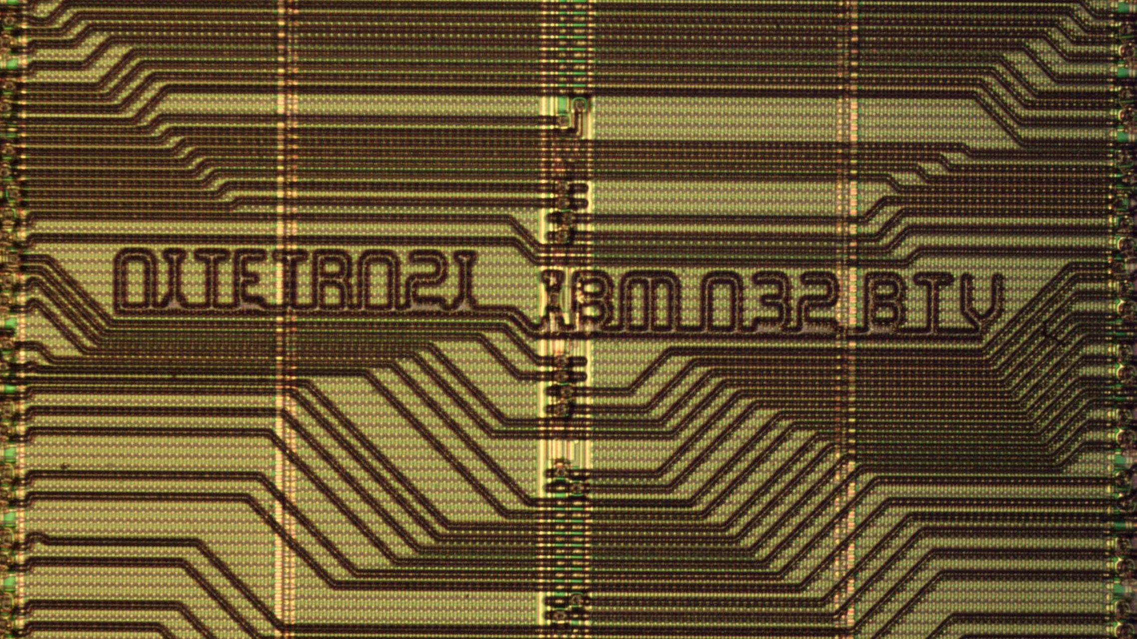
Although other manufacturers used integrated circuits for their third generation computers, IBM used modules called SLT (Solid Logic Technology), which were not quite integrated circuits. Each thumbnail-sized SLT module contained a few discrete transistors, diodes, and resistors on a square ceramic substrate. An SLT module was capped with a square metal case, giving it a distinct appearance. Although an SLT module doesn’t achieve the integration of an IC, it provides a density improvement over individual components. Each small SLT module was roughly equivalent to a complete SMS card, but much more reliable.7 By 1966, IBM was producing over 100 million SLT modules per year at a cost of 40 cents per module.6

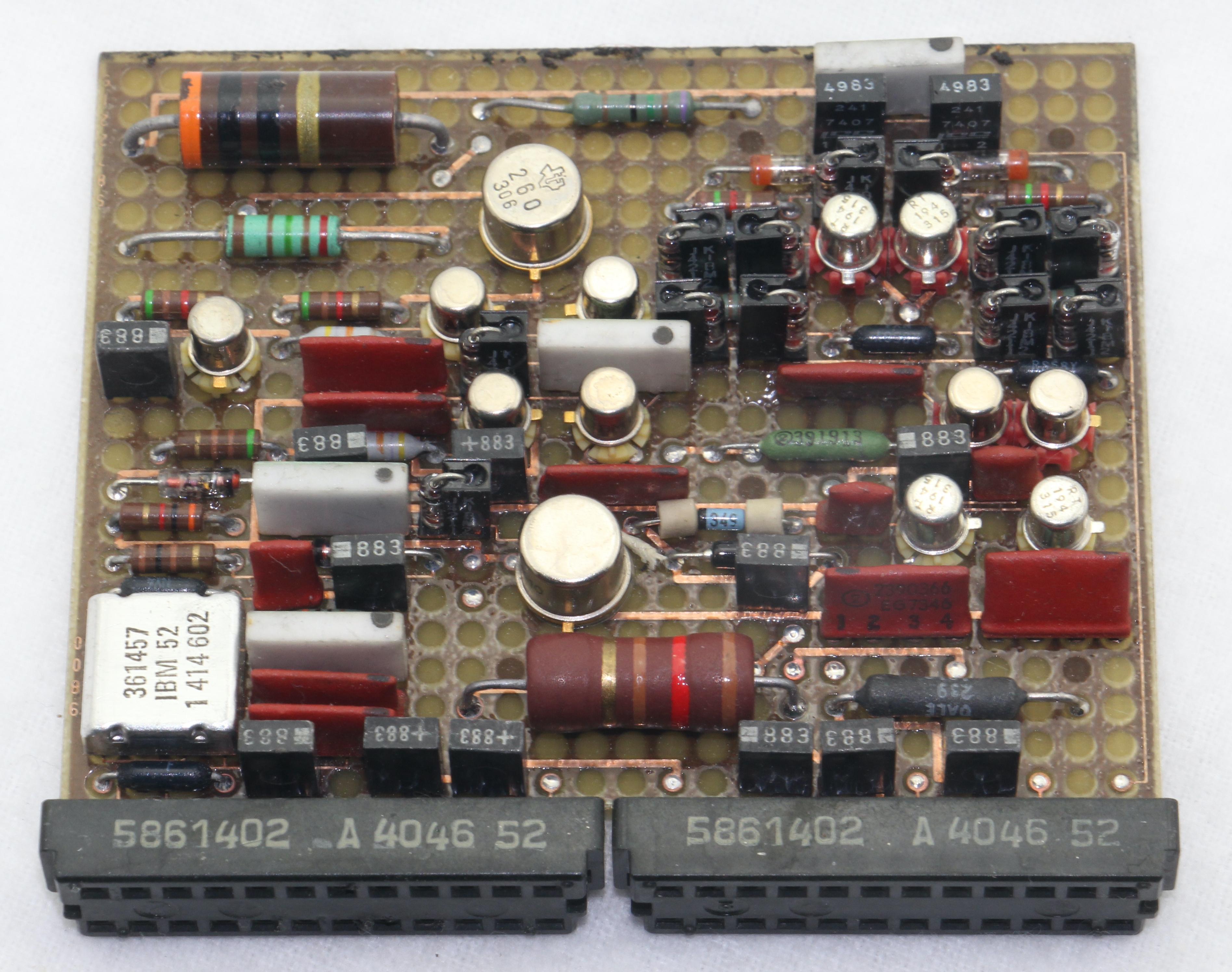
The board below is a logic board using 24 SLT modules. These modules implement AND-OR-INVERT logic gates, the primary logic circuit used in System/360. This board was probably part of the CPU.

A logic board using SLT modules. (The display box labeled this as an MST board though.)


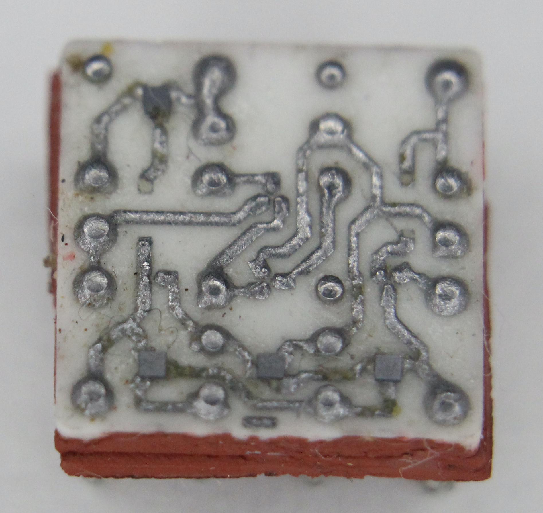
The photo below shows the circuitry inside an SLT module. This module has four transistors (the tiny gray squares). SLT modules typically include thick-film resistors, but none are visible in this module.

Closeup of an SLT module showing the tiny silicon dies mounted on the ceramic substrate.


The box also has an SLT card with analog circuitry (maybe for the computer’s core memory or power supply). This card has one SLT module, a simple module that contains four transistors (number 361457). I don’t know why this board has so many discrete transistors; perhaps they are higher-power transistors than SLT modules provided.

A card using an SLT module (the metal square in the lower left).

Integrated circuits: MST (Monolithic System Technology)

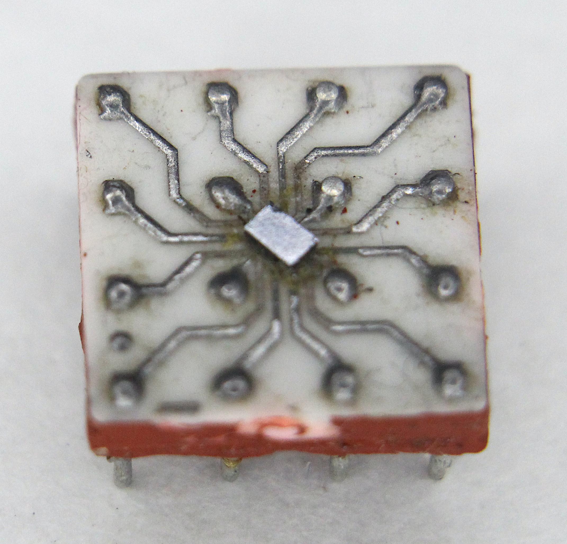
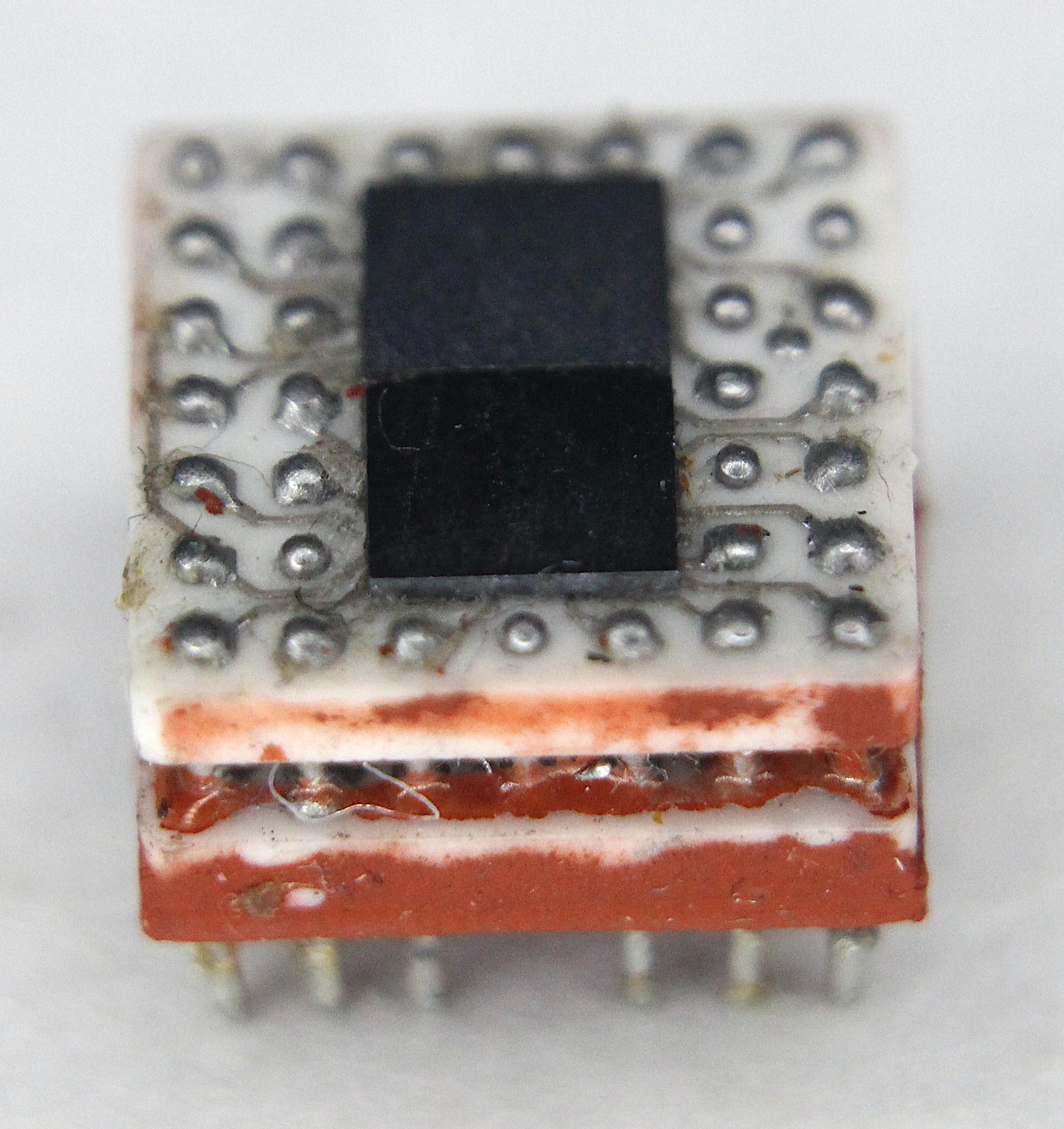
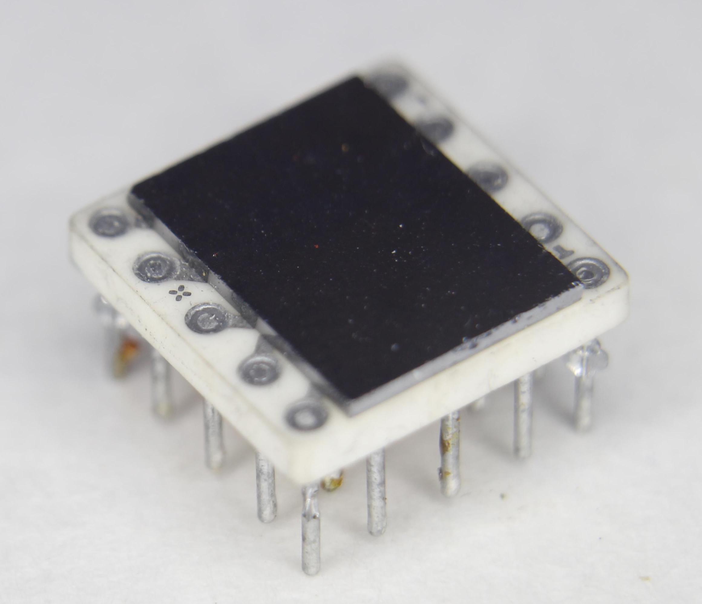
For a few years, IBM used SLT modules while other computer manufacturers used integrated circuits. Eventually, though, IBM moved to integrated circuits, which they called Monolithic System Technology (MST). An MST module looks like an SLT module from the outside, but inside it contains a monolithic die (i.e. an integrated circuit) rather than the discrete components of SLT. MST was first used in 1969 for the low-end System/3 computer.

An MST module looks like an SLT module from the outside, but has an integrated circuit die inside.


The photo above shows the box’s MST module. The silicon die is the tiny shiny rectangle in the middle, connected to the 16 pins of the module. The chip was mounted upside down, soldered directly to the substrate. This upside-down mounting is unusual; most other manufacturers used ceramic or plastic packages for integrated circuits, with the silicon die connected to the pins via bond wires.

Core memory

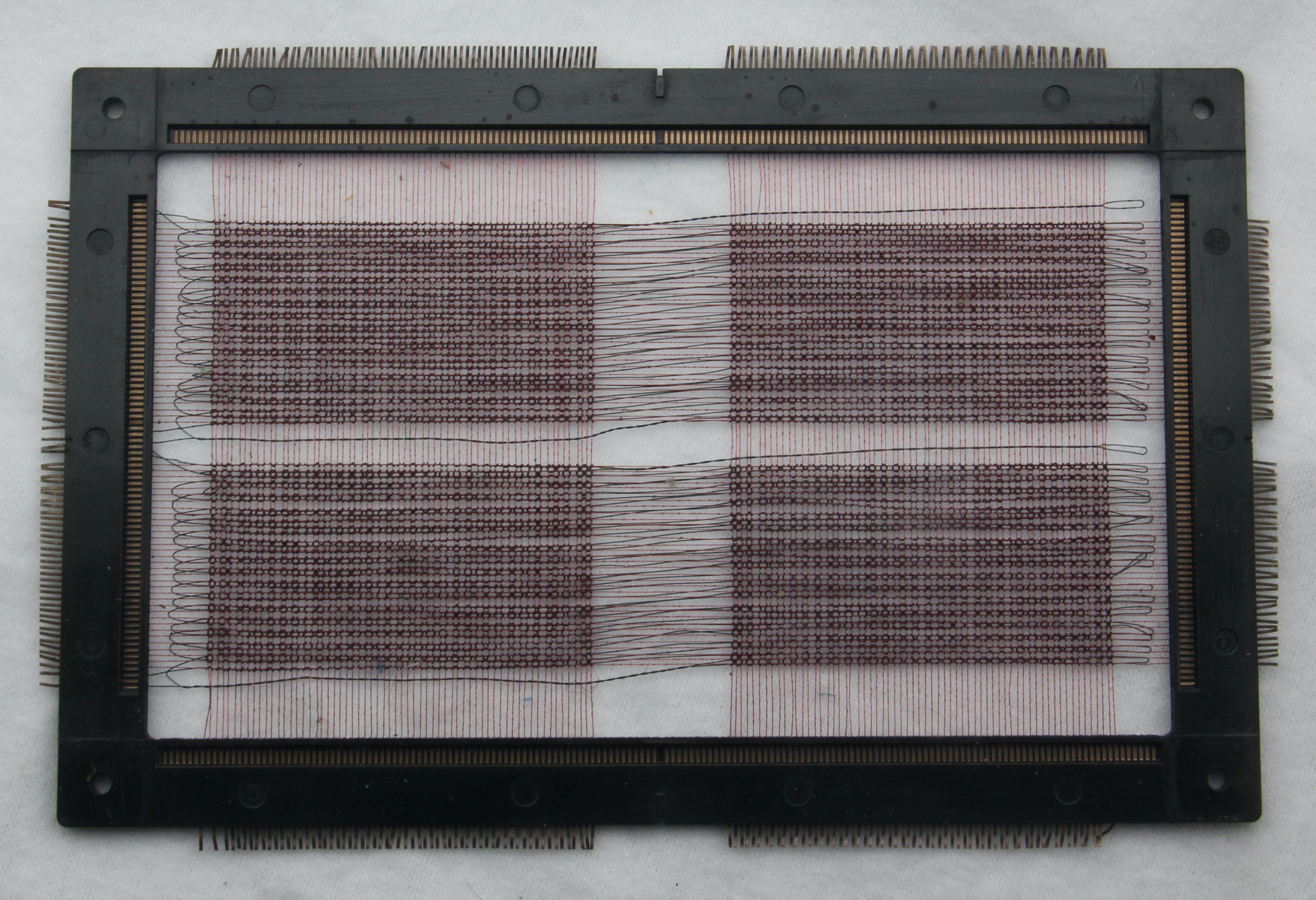
The box contains a core memory plane; most computers from the 1950s until the early 1970s used magnetic core memory for their main memory.8 This plane holds 8704 bits and is from a System/360 Model 20, the lowest-cost and most popular computer in the System/360 line.9

Core plane from a System/360 Model 20.


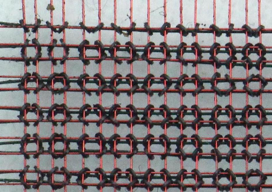
In core memory, each bit is stored in a tiny magnetized ferrite ring. The ferrite rings are organized into a matrix; by energizing a pair of wires, one bit is selected for reading or writing. Multiple core planes were stacked together to store words of data. Because each bit required a separate ferrite ring, magnetic core memory was limited in scalability. This opened the door for alternative storage approaches.

Closeup of the core plane, showing the wires through the tiny ferrite cores.

Semiconductor memory

IBM was an innovator in semiconductor memory and this is reflected in the numerous artifacts in the box that show off memory technology.10 Modern computers use a type of memory chip called DRAM (dynamic RAM), storing each bit in a tiny capacitor. DRAM was invented at IBM in 1966 and IBM continued to make important innovations in semiconductor memory.

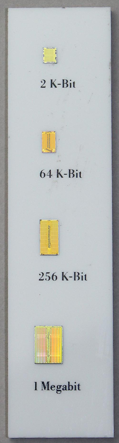
Although magnetic core memory was the dominant RAM storage technique in the 1960s, IBM decided in 1968 to focus on semiconductor memory instead of magnetic core. The first computer to use semiconductor chips for its main memory12 was the IBM System/370 Model 145 mainframe (1970). Each chip in that computer held just 128 bits, so a computer might need tens of thousands of these chips.11 Fortunately, memory density rapidly increased, as shown by the dies below. I’ll discuss the 2-kilobit chip in detail; my die photos of the others are in the footnotes13.

The box includes a display with four memory dies: 2 K-Bit, 64 K-Bit, 256 K-Bit, 1 Megabit.


The photo below shows the 2-kilobit die14 under a microscope. It is a static RAM chip from 1973, not as dense as DRAM since it uses six transistors per bit. The tiny white lines on the chip are the metal layer on top of the silicon, wiring the circuitry together. Around the outside of the die are 26 solder bumps for attaching the chip to the substrate. Note that this chip is mounted upside down (“flip-chip”) on the substrate, unlike most integrated circuits that use bond wires. The chip is covered with a protective yellowish film, except where the solder bumps are located.

Die photo of the 2-kilobit chip.


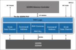
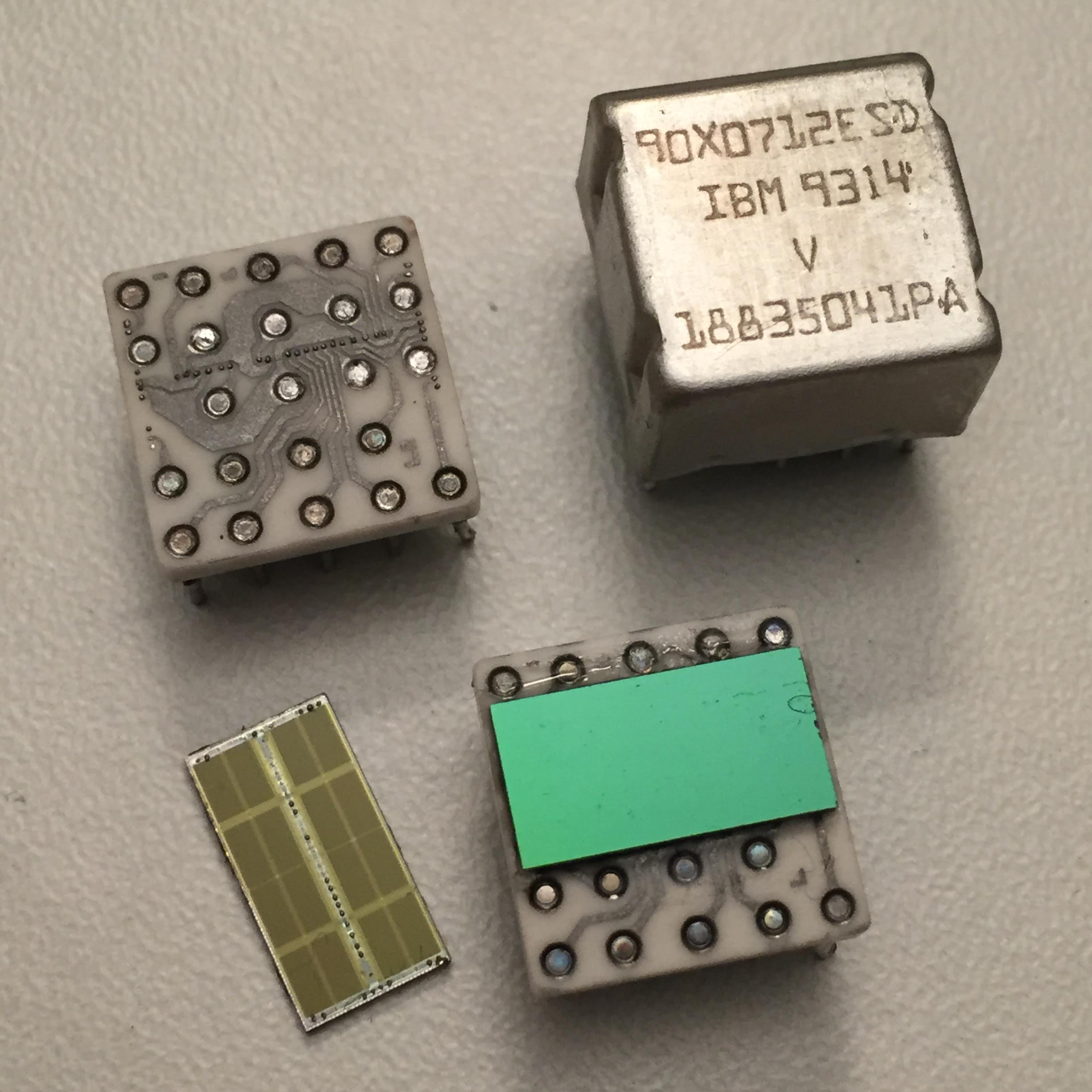
To increase the density of storage, four of these chips were mounted in a two-layer MST module, yielding an 8-kilobit module. The module in the box (below) has the square metal case removed, showing the silicon dies inside. These memory modules provided the main memory for the IBM System/370 models 115 and 125, as well as the memory expansion for the models 158 and 168 (1972).

The memory module has chips on two levels. This is an 8-kilobit module composed of four 2-kilobit chips.


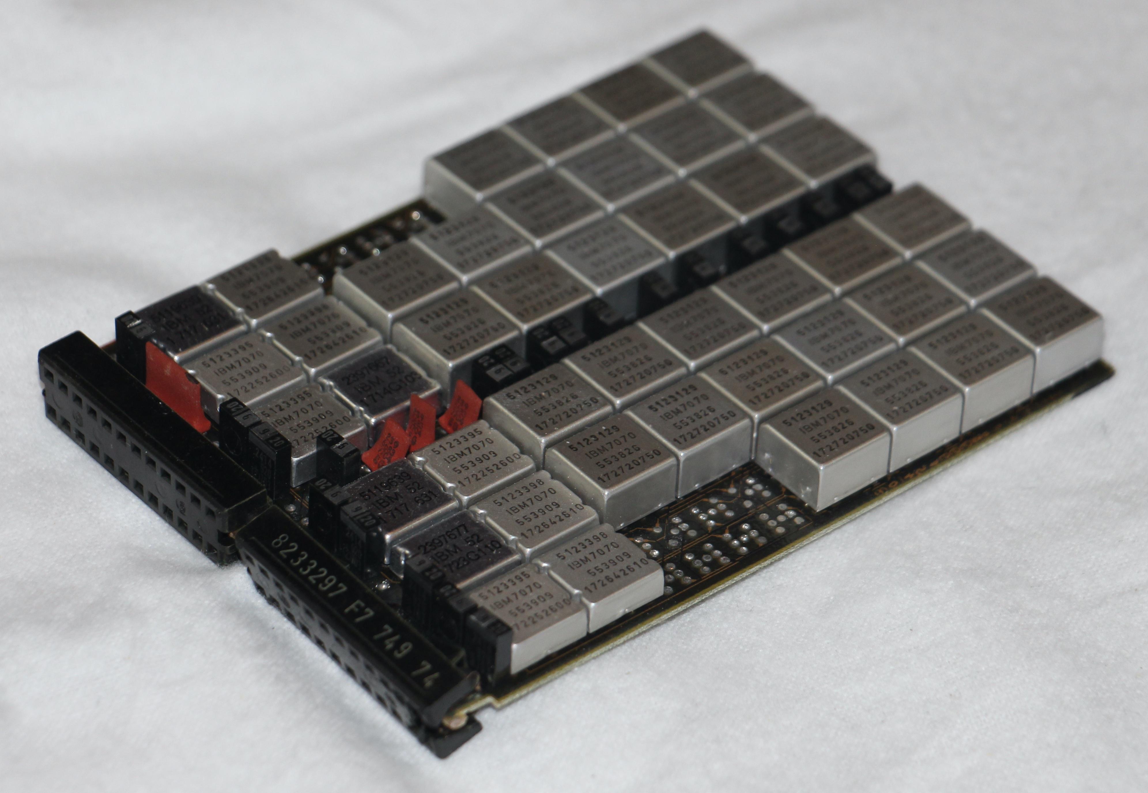
Each memory card (below) contained 32 of these modules to provide 32 kilobytes of storage. In the photo below, you can see the double-height memory modules along with shorter modules for support circuitry. A four-megabyte main memory unit held 144 of these cards in a frame about 3 feet × 3 feet × 1 foot, so semiconductor memory was still fairly bulky in 1972.

The memory board contains regular MST modules and double-height modules that hold the memory chips.


Moving along to some different memory chips, the box includes two silicon wafers holding memory dies, a 5″ wafer and a 4″ wafer.

The two silicon wafers.


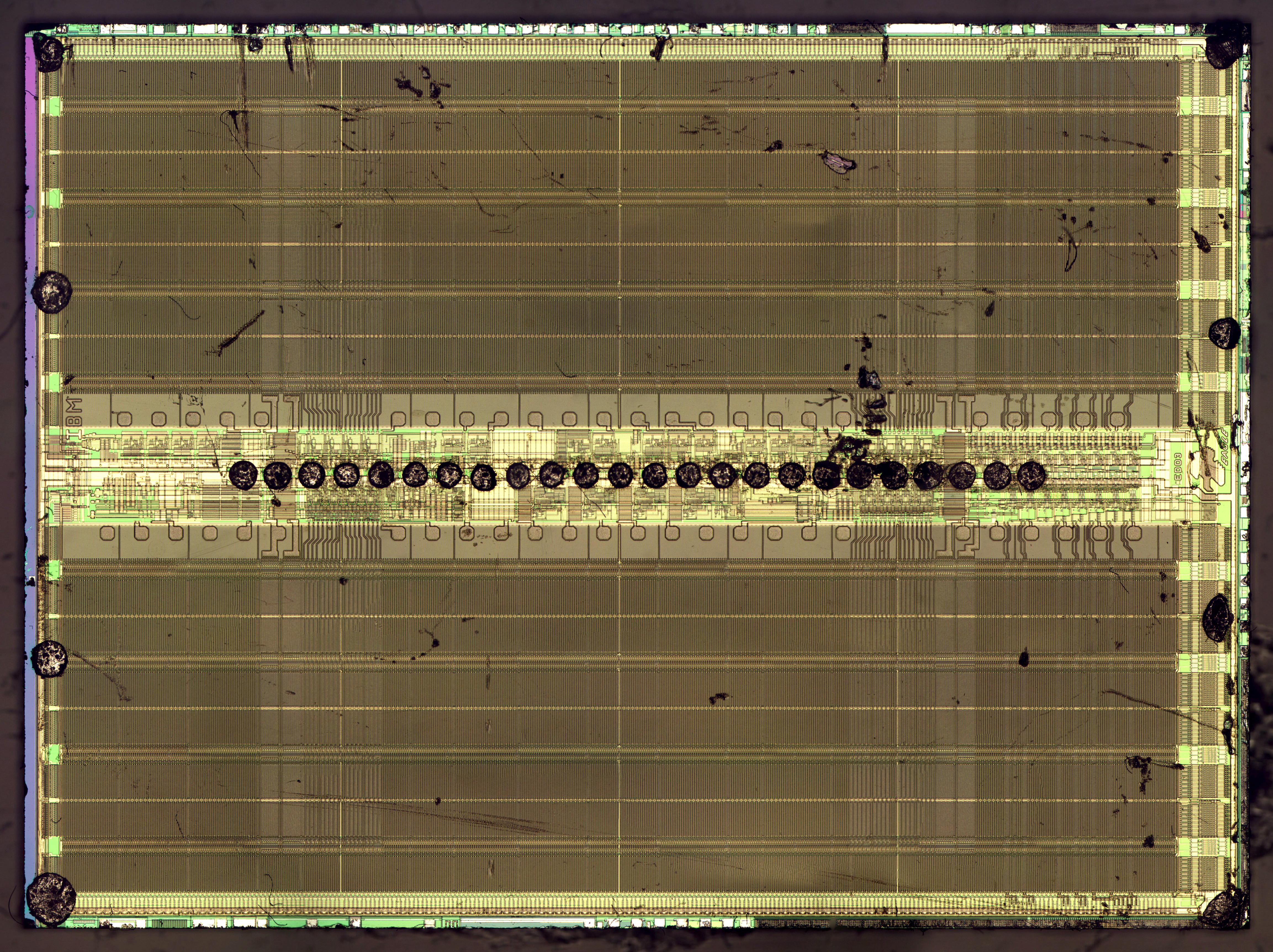
The smaller four-inch wafer (1982) holds 288-kilobit dynamic RAM chips, an unusual size as it isn’t a power of 2.15 The explanation is that the chip holds 32 kilobytes of 9-bit bytes (8 + parity). In the die photo, you can see that the memory array is mostly obscured by complex wiring on top of the die. This wiring is due to another unusual part of the chip’s design: for the most efficient layout, the memory bit lines have a different spacing from the bit decode lines. As a result, irregular wiring is required to connect the parts of the chip together, forming the pattern visible on top of the chip. Because this die is on the wafer, you can see the alignment marks and test circuitry around the outside of the chip.

Die photo of the 4″ wafer.


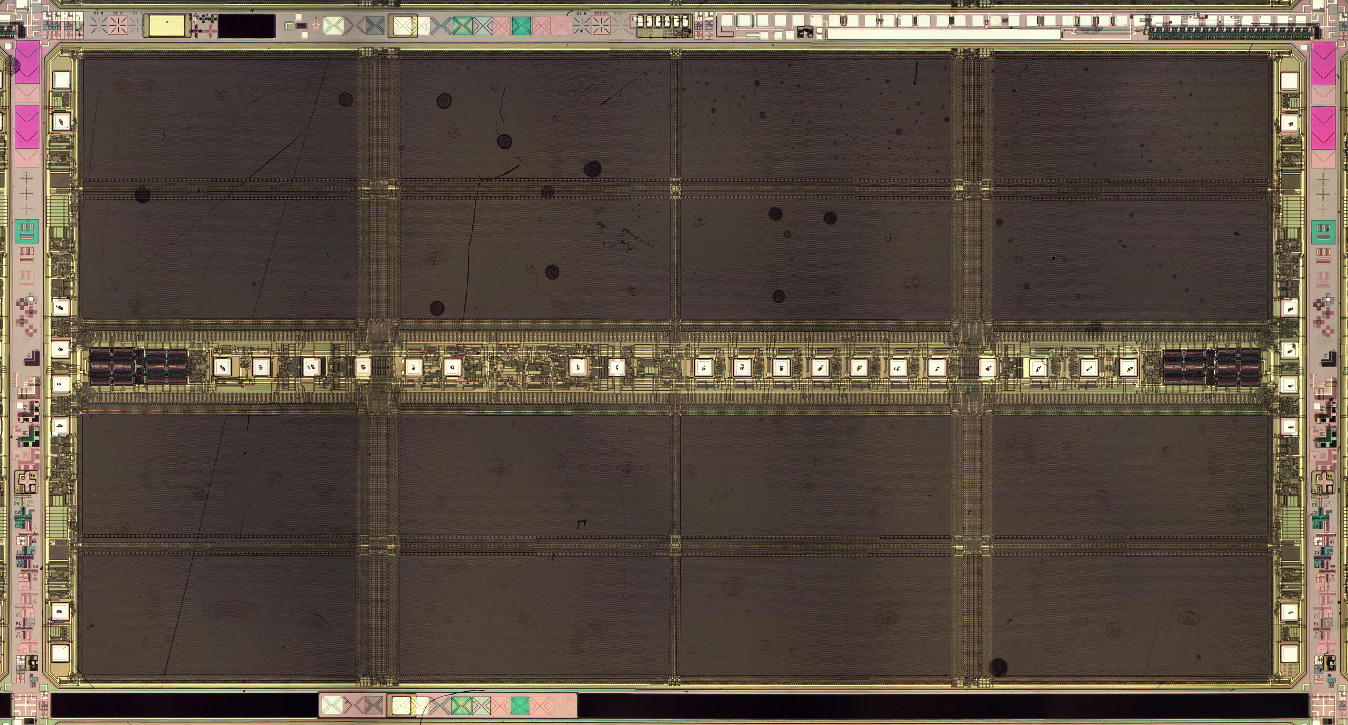
The five-inch wafer holds 1-megabit memory chips16 that were used in the IBM 3090 mainframe17 (1985). This computer used circuit cards with 32 of these chips, providing four megabytes of storage per card, a huge improvement over the 32-kilobyte card described earlier. The 3090 used multiple memory cards, providing up to 256 megabytes of main storage. The die photo below shows how the chip consists of 16 rectangular subarrays, each holding 64 kilobits.

Die photo of the 1-megabit DRAM chip on the 5″ wafer. The dark circles are dirt, not solder balls.


The photo below shows how this die is mounted upside-down on the ceramic substrate with the solder bumps connected to the 23 pins of the module. This module (not part of the box) was used in the IBM PS/2 personal computer.18 The die below looks green, unlike the die above, but that’s just due to the lighting.

Construction of an IBM memory module. This module was not part of the box, but the die is the same as the 5″ die. Photo courtesy of Antoine Bercovici.


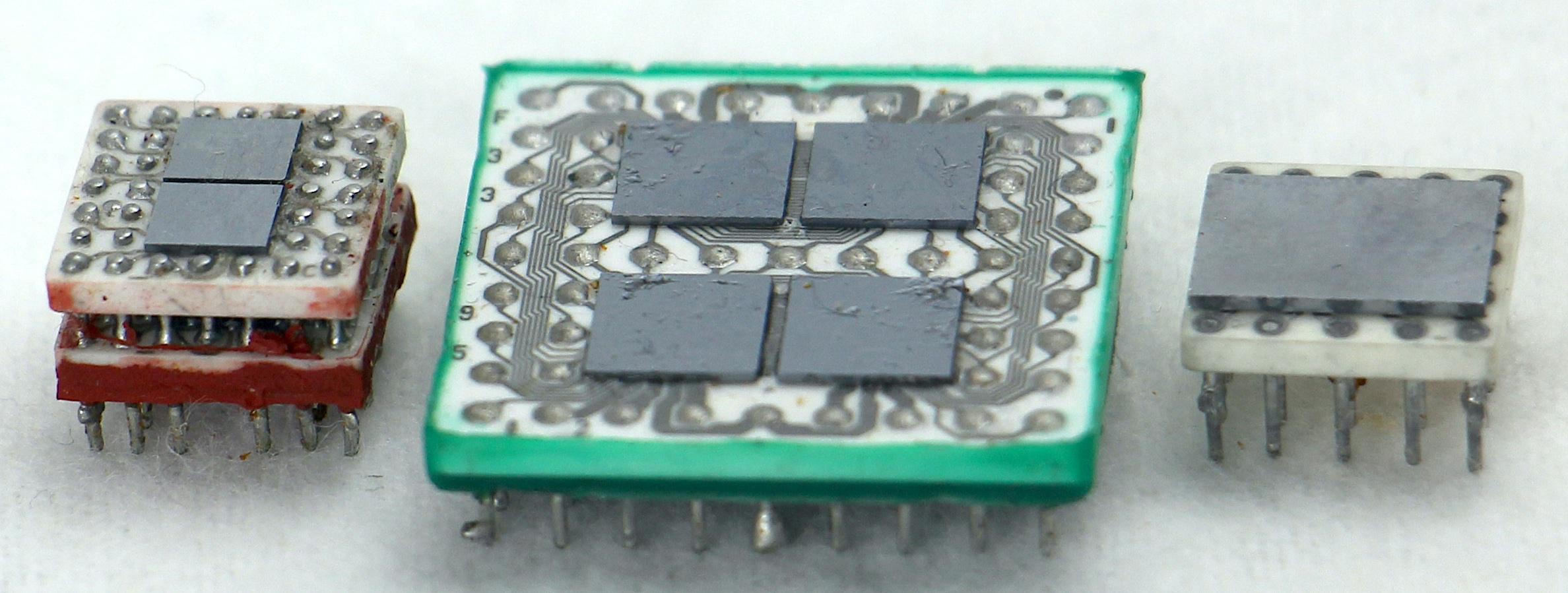
The photo below compares three memory modules from the technology box. The first module is the 8-kilobit module containing four 2-kilobit chips, described earlier. The second module is a much wider 512-kilobit module, built from four 128-kilobit dies. The third module contains a 1-megabit chip (the one in the 4-chip display, not from the wafer). These megabit modules were used in the IBM 3090 mainframe’s secondary storage.

Three memory modules: 8-kilobit, 512-kilobit, and 1-megabit.

Disk platter

The box contains a segment of a 14″ IBM disk platter, used in disk storage systems from minicomputers to mainframes. IBM was a pioneer in hard disks, starting with the IBM RAMAC (1956), which weighed over a ton and held 5 million characters on a stack of 24″ platters. IBM switched to 14″ platters in 1961 and by 1980 the IBM 3380 disk system held up to 2.5 gigabytes in a large cabinet of 14″ platters.19 The 14″ platter was also popular in low-cost, removable disk cartridge (1965) used with many minicomputers. The 14″ disk platter was finally replaced by an 11″ platter with the introduction of the IBM 3390 disk drive in 1989. Nowadays, laptops typically use 2.5″ platters; amazingly, disk capacity kept increasing as disk diameter steeply decreased.

Section of a 14″ disk platter from the display box.

Artifacts from the IBM 3090

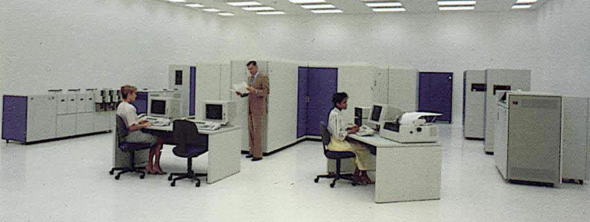
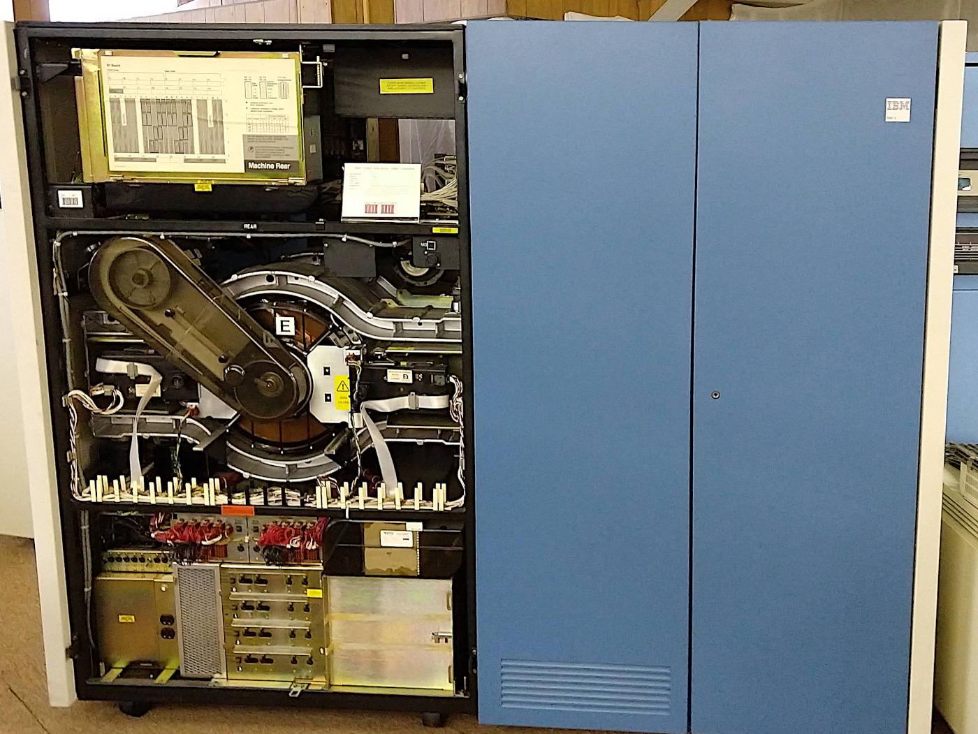
At the time of the box’s creation, the 3090 mainframe was IBM’s new high-performance computer (below), so the box has several artifacts that show off the technology in this computer. Although the IBM 3090 (1985) had top-of-the-line performance at the time, by 1998 an Intel Pentium II Xeon microprocessor had comparable performance,20 illustrating the remarkable improvements of microprocessor technology.

An IBM 3090 data center. Photo from the IBM 3090 brochure.


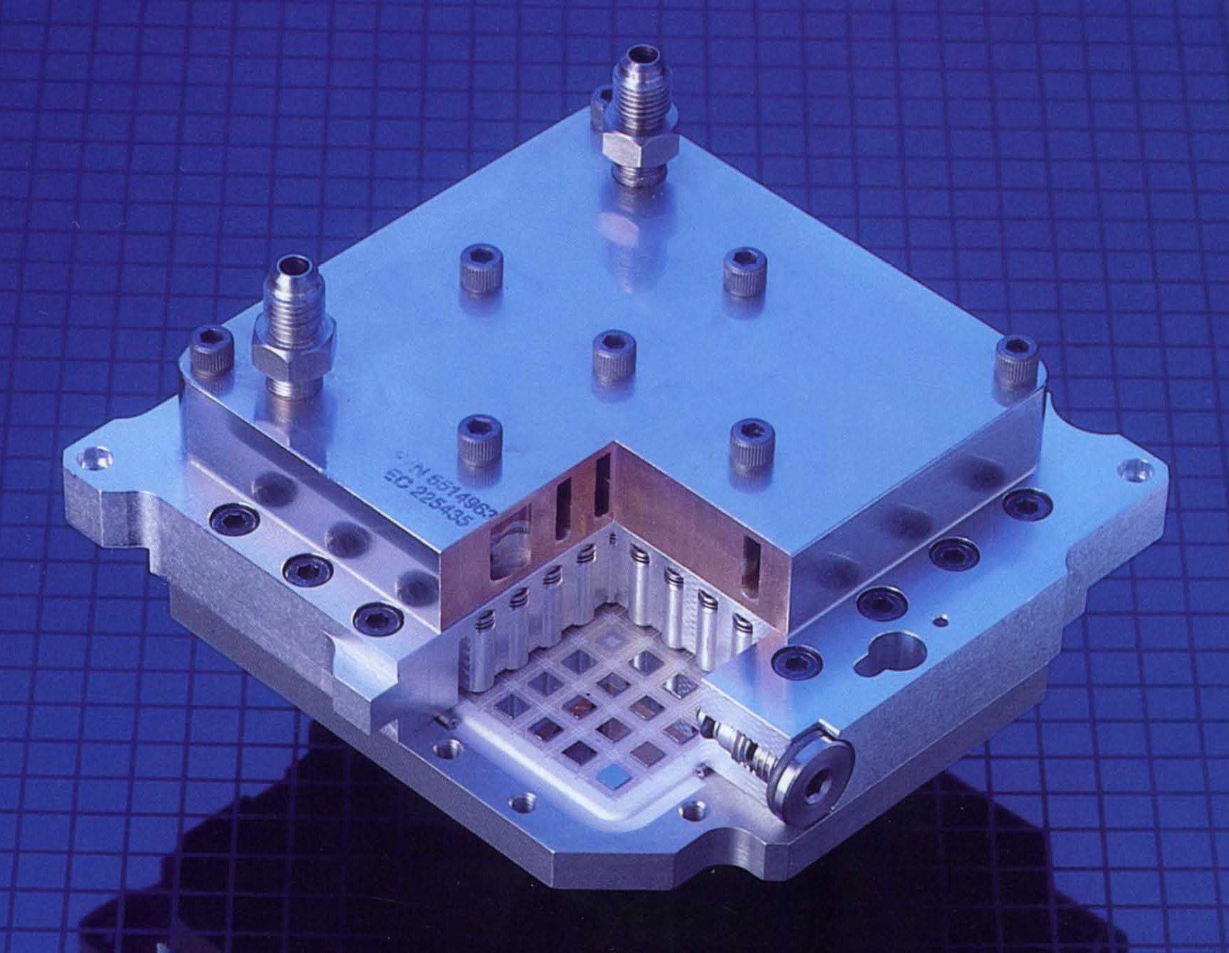
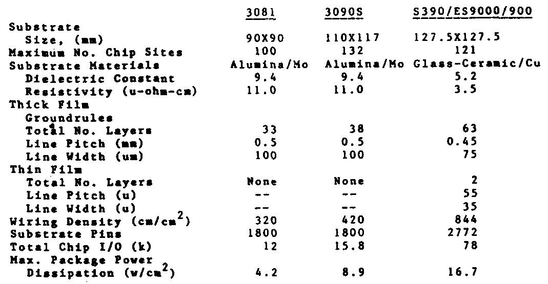
In 1980, IBM introduced the thermal conduction module (TCM), an advanced way to package integrated circuits at high density, while removing the heat that they generate.21 A TCM starts with a multi-chip module with about 100 high-speed integrated circuits mounted on a ceramic substrate, as shown below. This substrate contains dozens of wiring layers to connect the integrated circuits.22 To remove the heat, the ceramic substrate is packaged in a TCM, which has a metal piston contacting each silicon die. These pistons are surrounded by helium (which conducts heat better than air), and the whole TCM package is water-cooled. Finally, nine TCMs are mounted on a printed circuit board.

The hierarchy of components in the IBM 3090: chips are mounted on a ceramic substrate, which is assembled into a TCM. A board holds nine TCMs.


This incredibly complex heat-removal system was required because the 3090 used emitter-coupled logic (ECL), the same type of circuitry used in the Cray-1 supercomputer. Although ECL is a very fast logic family, it is also power-hungry and generates much more heat than the MOS transistors used in microprocessors.

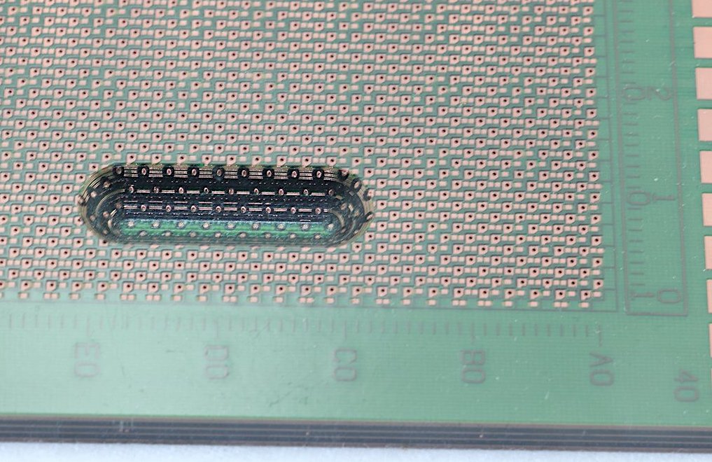
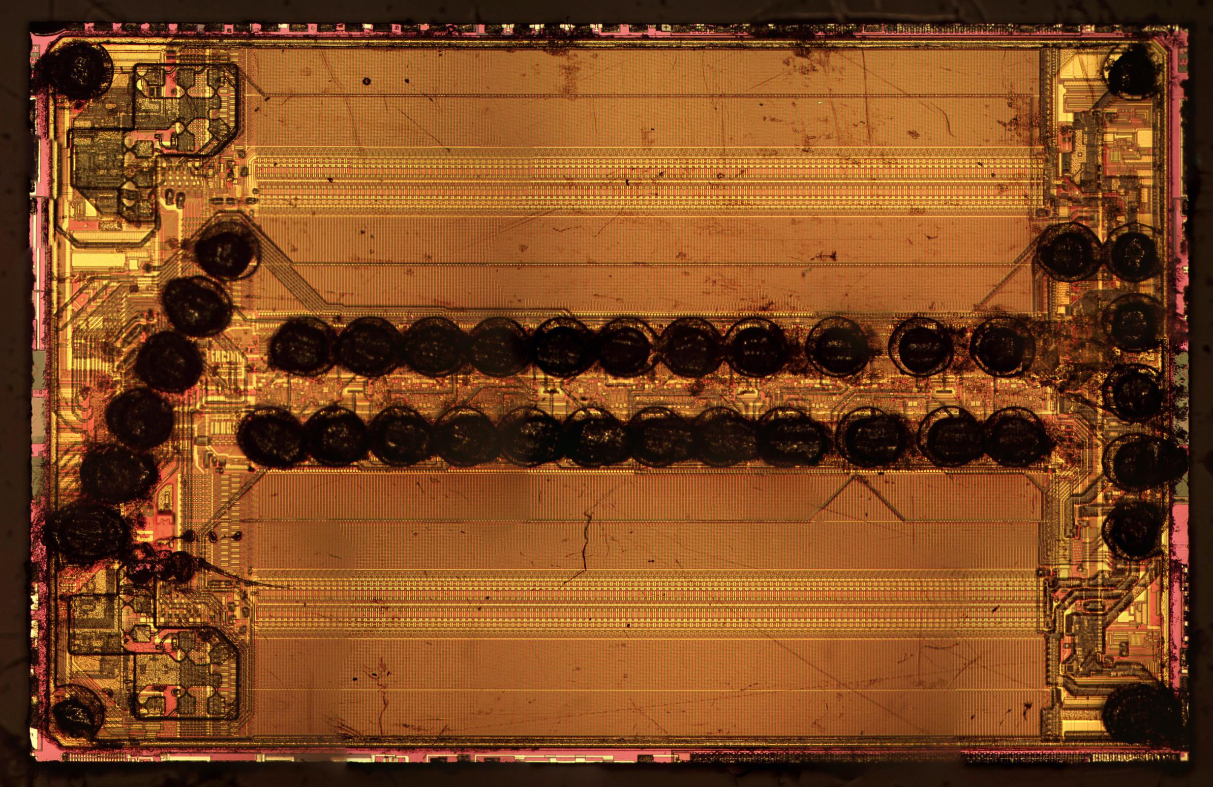
The ceramic substrate for a TCM, from the box. It is fairly small, measuring 11×11.7 cm. This substrate holds 100 silicon dies; one is visible near the middle.


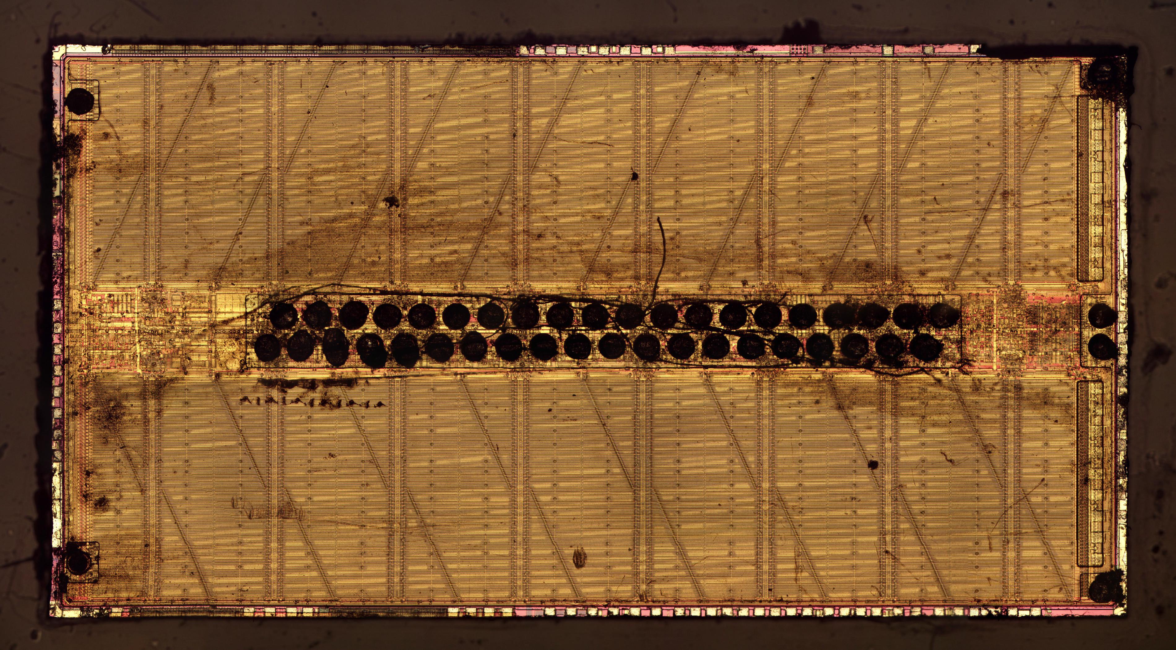
The photo above shows the ceramic substrate. Normally, the substrate has 100 silicon dies mounted on it, but this sample has just a single die. The box also includes a cross-section slice of the ceramic substrate (below). This shows the 38 layers of wiring inside the substrate, as well as the pins on the underside.

Cross-section of the ceramic substrate, showing the multiple layers of internal wiring.


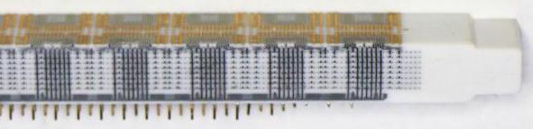
Each TCM had 1800 pins so it could be plugged into a printed circuit board and connected to the rest of the system. Each board held 9 TCMs and was powered with an incredible 1400 amps. The box includes a PCB sample, showing its multi-layer construction (below), and the dense grid of holes to receive the ceramic substrate.

Closeup of the printed circuit board used in the IBM 3090. The routed groove shows the multi-layer construction.


Finally, here’s a nice cutaway of a TCM from the detailed IBM 3090 brochure. At the bottom, it shows the silicon dies mounted on the ceramic substrate. The dies are contacted by the heat sink pistons in the middle. The connections on top are for the cooling water.

This cut-away image from IBM shows the internal construction of a TCM.


Conclusion

This technology exhibit box was created 35 years ago. Looking at it from the present provides a perspective on the history of both IBM and the computer industry. The box’s date, 1986, marks the peak of IBM’s success and influence,23 right before microcomputers decimated the mainframe market and IBM’s dominance. What I find interesting is that the technology box focuses on mainframes and lacks any artifacts from the IBM PC (1981), which ended up having much more long-term impact..24 This neglect of microcomputers reflects IBM’s corporate focus on the mainframe market rather than the PC market (which, ironically, IBM created).

In the bigger historical picture, the technology box covers a time of great upheaval as electromechanical accounting machines were replaced by three generations of computers in rapid succession: vacuums tubes, then transistors, and finally integrated circuits. In contrast to this period of rapid change, nothing has replaced integrated circuits over the past 50 years. Instead, integrated circuits have remained, but improved by many orders of magnitude, as described by Moore’s Law. (Compared to the room-filling IBM 3090 mainframe, an iPhone has 1000 times the performance and 50 times the RAM.) Will integrated circuits continue their dominance for the next 50 years or will some new technology replace them? It remains to be seen.

Thanks to Cyprien for providing this amazing box of artifacts. I announce my latest blog posts on Twitter, so follow me @kenshirriff. I also have an RSS feed.

Notes and references

  1. The box was apparently created in Stuttgart, Germany. The components are protected by a piece of plexiglass, with labels in German for all the components, such as Mehrschicht-Keramiktrager for multi-layer ceramic substrate. The labels are listed here if you’re interested.
    The box is labeled in German: “Computertechnologie”.


    The box originally included several German books on computer technology but since they are missing I had to do some research and come up with my own narrative.

  2. For more information on the pluggable tube modules, see the schematics of IBM’s pluggable units (which lack the box’s MS-7A module). (I suspect the MS-7A was selected for the box because it is more compact than most of the pluggable modules, having one layer of circuitry below the tube, rather than two.)
  3. The IBM 604 service manual says that the thyratron tube modules are designated TH, but the module in the box is designated MS-7A. I don’t know why the designations don’t match up.
  4. People sometimes think that an 8-tube module held a byte. This is wrong for two reasons. First, bytes didn’t exist back then. IBM’s early scientific computers used 36-bit words, while the business computers were based on characters of 6 bits plus parity. Second, 8 tubes didn’t correspond to 8 bits because circuits often required multiple tubes. For instance, a tube module could implement three bits of register storage.
  5. The SMS card in the box is type AXV, a complementary emitter follower circuit used in the IBM 1443 printer and other systems.
  6. SLT was controversial, since other companies used more-advanced integrated circuits rather than hybrid modules. In typical IBM fashion, the vice president in charge of SLT was demoted in 1964, only to be reinstated in 1966 when SLT proved successful. My view is that integrated circuit technology was too immature when the System/360 was released, so IBM’s choice to use SLT made the System/360 possible. However, it only took a year before integrated circuits became practical, as shown by their use in competing mainframes. I think IBM stuck with SLT modules longer than necessary. Integrated circuits rapidly increased in complexity (Moore’s Law), while SLT modules could only increase density through hacks such as putting resistors on the underside (SLD) and using two layers of ceramic (ASLT).
  7. Curiously, this card is labeled in the box as an MST card, but checking the part numbers shows it has SLT modules. Specifically, it contains the following types of SLT modules (click for details): 361453 AND-OR-Invert, 361454 inverters, 361456 AND-OR-extender, and 361479 inverters. The SLT modules are also documented in IBM’s manual.
    Schematic of one of the SLT modules on the board (361453 AND-OR-INVERT (AOI) gate) from the IBM manual.


    The schematic above shows one of the SLT modules. (IBM had their own symbol for transistors; T1 is an NPN transistor.) This gate is built from diode-transistor-logic, so it’s more primitive than the TTL logic that became popular in the late 1960s. The “Extend” pins are used to connect modules together to build larger gates, so the modules provide a lot of flexibility. This module inconveniently requires three voltages. This SLT module contained one transistor die, three dual-diode dies, and three thick-film resistors. During manufacturing, the resistors were sand-blasted to obtain accurate resistances, an advantage over the inaccurate resistances on integrated circuit dies.

  8. The System/360 line was designed as a single 32-bit architecture for all the models. The Model 20, however, is a stripped-down, 16-bit version of System/360, incompatible with the other machines. (Some people don’t consider the Model 20 a “real” System/360 for this reason.) But due to its low price, the Model 20 was the most popular System/360 with more than 7,400 in operation by the end of 1970.
  9. This core memory plane from a System/360 Model 20 is a 128×68 grid. Note that this isn’t a power of 2: the plane provided 8192 bits of main memory storage as well as 512 bits for registers. Using the same core plane for memory and registers hurt performance but saved money. The computer used five of these planes to make a 4-kilobyte memory module, or 10 planes for an 8-kilobyte module. For details, see the Model 20 Field Engineering manual.
  10. For an extensive list of references on DRAM chips, see the thesis Impact of processing technology on DRAM sense amplifier design (1990). For a history of memory development at IBM through 1980, from ferrite core to DRAM, see Solid state memory development in IBM.
  11. The System/370 Model 145 was the first computer with semiconductor main memory. Each thumbnail-sized MST module held four 128-bit chips; 24 modules fit onto a 12-kilobit storage card. A shoebox-sized Basic Storage Module held 36 cards, providing 48 kilobytes of storage with parity. By modern standards this storage is incredibly bulky, but it provided twice the density of the magnetic core memory used by contemporary systems. The computer’s storage consisted of up to 16 of these boxes in a large cabinet (or two), providing 112 kilobytes to 512 kilobytes of RAM.
    Photos showing the 512-bit memory module, the 12-kilobit memory card, and the 48-kilobyte basic storage module. Photos from IBM 370 guide.
  12. IBM had used monolithic memory for special purposes earlier, holding the “storage protect” data in the IBM 360/91 (1966) and providing a memory cache in the System/360 Model 85.
  13. I wasn’t able to find exact details on the 64-kilobit, 256-kilobit, and 1-megabit chips from the display, but I took die photos.
    Die photo of the 64k memory chip.


    The 64-kilobit chip is shown above. The solder balls are the most visible part of the chip. The article A 64K FET Dynamic Random Access Memory: Design Considerations and Description (1980) describes IBM’s experimental 64-kilobit DRAM chip, but the chip they describe doesn’t entirely match the chip in the box. There were probably some significant design changes between the prototype chip and the production chip.

    Die photo of the 256-kilobit RAM, roughly 1985.


    The 256-kilobit die is shown above. The diagonal lines on the die are similar, but not identical, to the die in A 256K NMOS DRAM (1984). That chip was designed at IBM Laboratories in Böblingen, Germany, and could provide 1, 2, or 4 bits in parallel.

    Die photo of the 1-megabit memory chip.


    The 1-megabit die is shown above. IBM was the first company to begin volume production of 1-megabit memory chips and the first company to use them in mainframe computers. This chip was used in the IBM 3090 mainframe, but was later replaced by the faster and smaller “second-generation” 1-megabit chip on the 5″ wafer. One interesting feature of this die is the “eagle” logo, shown below.

    The eagle chip art on the 1-megabit RAM chip, slightly scratched.


    The box includes a 1-megabit MST module (below) that uses this chip. Because the chip’s solder balls are along its center, the module omits the center three pins to make room for the connections to the chip.

    The 1-megabit chip mounted in an MST module.


  14. This memory card and its 2-kilobit chips are described in detail in A High Performance Low Power 2048-Bit Memory Chip in MOSFET Technology and Its Application (1976). These modules were used in the main memory of the IBM System 370 models 115 (1973) and 125 (1972) as well as upgraded memory for the models 158 (1972) and 168 (1972). The IBM System/360 Model 138 (1976) and Model 148 (1976) also used 2K MOSFET chips, presumably the same ones. The 2-kilobit chip was developed at IBM Laboratories in Böblingen, Germany; this may have motivated its inclusion in this German display box.
    Closeup of the 2-kilobit RAM chip.


    The closeup of the 2-kilobit die shows some of the decoder circuitry (left) and the storage cells (right). Two solder balls are in the lower left; the rest of the die is covered with a protective yellow film, probably polyimide. Each storage cell consists of six transistors. The chip is built with metal-gate NMOS transistors.

  15. The 288-kilobit chip is described in detail in A 288Kb Dynamic RAM.
    Closeup of the IBM 288-kilobit memory chip showing the programmable fuses.


    The closeup die photo above shows some of the memory cells (at the top and bottom), wired into bit lines. One unusual feature of this chip is that has redundancy to work around faults. In particular, four redundant word lines can be substituted for faulty ones, by blowing configuration fuses. I think the large boxes with circles in the middle are four of the fuses.

    The part number on the 4″ die: OITETR02I IBM 032 BTV.


    The photo above shows the chip’s part number; BTV refers to IBM’s Burlington / Essex Junction, VT semiconductor plant where the chip was designed. This plant was acquired by GlobalFoundaries in 2015. This photo also shows the complex geometrical wiring, unlike the regular matrix in most memory chips.

  16. Note that there are two 1-megabit chips in the box. The chip on the 4-chip display is an older chip than the one on the 5″ wafer. The 1-megabit memory chip on the wafer is described in An Experimental 80-ns l-Mbit DRAM with Fast Page Operation (1985). It uses a single 5-volt power supply. The chip is structured as four 256-kbit quadrants, each subdivided into four 64-kbit subarrays. It has two redundant bit lines per quadrant for higher yield. The horizontal solder balls through the middle of the chip are the common connections for each quadrant, while the vertical connections along the left and right edges provide the signals specific to each quadrant. This quadrant structure allows the chip to be accessed as 256K×4 or 1M×1.
  17. IBM’s overview of the 3090 family provides details on the hardware, including the memory and TCM modules. Page 10 discusses IBM’s memory technology as of 1987 and has a picture of their “second generation” 1-megabit chip, which matches the die on the 5″ wafer.
  18. The 1-megabit memory chips were used in the IBM 3090 mainframe, but I think the faulty ones were used in IBM PS/2 personal computer. You can see the unusual metal MST packages on many PS/2 cards. Specifically, if one of the four quadrants in the memory chip had a fault, the memory chip was used as a 3/4-megabyte chip. These had four part numbers, depending on the faulty quadrant: 90X0710ESD through 90X0713ESD (ESD probably stands for Electrostatic Sensitive Device). The PS/2 2-megabyte memory card (90X7391) had 24 chips providing 2 megabytes with parity. The board used chips with alternating bad banks so the memory regions fit together.
  19. Since several of the artifacts in the box came from the IBM 3090 mainframe, and the 3380 disk system was used with the 3090 mainframe, my suspicion is that the platter is from the 3380 disk system, shown below.
    An IBM 3380E disk storage system, holding 5 gigabytes. The disk platters are center-left, labeled “E”. Photo taken at the Large Scale Systems Museum.


  20. It’s difficult to precisely compare different computers, especially since the 3090 supported multiple processors and vector units. I looked at benchmarks from 2001 comparing various computers on a linear algebra benchmark. The IBM 3090 performed at 97 to 540 megaflops/second for configurations of 1 to 6 processors respectively. An Intel Pentium II Xeon performed at 295 megaflops/second, a bit faster than the 3-processor IBM 3090. To compare clock speeds, the IBM 3090 ran at 69 MHz, while the Pentium ran at 450 MHz. An IBM 3090 cost $4 million while a Pentium II system was $7,000 to $20,000. The IBM 3090 came with 64 to 128 megabytes of RAM while people complained about the Pentium II’s initial 512-megabyte limit. The point of this is that while the IBM 3090 was a powerful mainframe in 1985, microprocessors caught up in about 13 years, thanks to Moore’s Law.
  21. The table below compares characteristics of the Thermal Conduction Modules used in the IBM 3081 (1980), IBM 3090 (1985), and IBM S/390 (1990) computers. The board-level technology progressed similarly. For instance, a 3081 board took up to 500 amps, while a 3090 board took 1400 amps, and an S/390 board took 3400 amps.


    The IBM 4300-series processors (1979) used a ceramic multi-chip module that held 36 chips, but it used an aluminum heat sink and air cooling instead of the more complex water-cooled TCM. The IBM 4381‘s smaller multi-chip module is often erroneously called a TCM by online articles, but it’s a multilayer ceramic multichip module (MLC MCM). For more information about IBM’s chip packaging, see this detailed web page.

  22. For more information on TCMs, see the EEVblog teardown.
  23. Desktop computer sales first exceeded mainframe computer sales in 1984. Counting the number of employees, IBM peaked in 1985 and declined until 1994 (source). 1985 was also a peak year for IBM’s revenue and profits, according to The Decline and Rise of IBM. By 1991, IBM’s problems were discussed by the New York Times. After heavy losses, IBM regained profitability and growth in the 1990s, but never regained its dominance of the computer industry.
  24. Perhaps one reason that the technology box ignores IBM’s personal computers is that these computers didn’t contain IBM-specific hardware that they could show off: Intel built the 80×86 processor, while companies such as Texas Instruments built the memory and support integrated circuits. The lack of IBM-specific technology in these personal computers is one factor that led to IBM losing control of the PC-compatible market.

How Airshield Can Save Transportation

How Airshield Can Save Transportation
by Roger C. Lanctot on 01-31-2021 at 6:00 am

How Airshield Can Save Transportation

The COVID-19 pandemic has devastated public transportation of every variety from buses and taxis to airplanes and trains. The combination of remote work and evolving economic shutdowns impacting restaurants, entertainment venues, schools, and tourism have sapped transportation demand while mitigation measures have reduced supply.

Restoring the supply of transportation as economies emerge from the coronavirus crisis in the wake of widespread vaccine deployment will call for a corresponding restoration in confidence. Returning public transportation users on trains and planes and other means of conveyance will be looking for accomodations intended to combat present and future viral transmission among passengers. Many bus drivers, for example, have seen protective barriers installed.

Much has been made of research studies showing the prophylactic effect of airflow in taxis, trains, buses and airplanes. But these studies tend to look at the prevailing airflow – normally ceiling-to-floor and front-to-back in shared transit situations – the nature of air filtration and the frequency of cabin air replacement. (Taxis or shared cars are more complicated.)

Some of these studies consider the disruption of the prevailing airflow due to the presence and movement of human beings – the passengers and/or attendants.  Little effort has gone into actually modifying the airflow in order to use it as a more active defense against viral transmission.

Airshield, a retrofit device for airplanes, is intended to actually use airflow as a barrier to viral transmission in airplanes. Developed by Teague, a design firm focused on user experiences in the transportation industry, Airshield is intended as an inexpensive adaptation of existing cabin air exchange systems to provide individualized and inobtrusive protection to airplane passengers – even those sitting in close proximity.

I have flown three domestic flights since the onset of the pandemic. I can personally attest to the fact that flights during the COVID-19 pandemic are almost universally completely full and the airlines have done little to modify the in-cabin experience to inspire passenger confidence.

The airline I fly most frequently is United, United touts its award winning United CleanPlus program saying: “United is the first airline among the four largest U.S. carriers to be awarded Diamond status by APEX Health Safety powered by SimpliFlying for our cleanliness and sanitation efforts.”

United CleanPlus addresses the cleanliness of the airplane. It does not address the real threat of airborne viral transmission in flight.

United is not alone. The manufacturers of the airplanes themselves appear to be in a bit of denial. Writes Boeing:

“What happens when someone coughs next to other passengers on an airplane?  New Boeing research shows the cabin environment significantly reduces and removes those cough particles from the air.

“In fact, Boeing researchers say the design of the cabin and the airflow system create the equivalent of more than 7 feet (2 meters) of physical distance between every passenger—even on a full flight. The findings, along with the use of face coverings, enhanced cleaning and other safeguards lower the risk of passengers contracting COVID-19 during air travel.”

Boeing’s claims fly in the face of existing research. Notes a comment on the MIT Medical Website:

“Still, the design of air-handling systems on commercial aircraft makes it unlikely that you’ll be breathing in air from anyone more than a few rows away. In fact, a 2018 study that examined the transmission of droplet-mediated respiratory illnesses during transcontinental flights found that an infectious passenger with influenza or another droplet-transmitted respiratory infection was highly unlikely to infect passengers seated farther away than two seats on either side or one row in front or in back.”

These findings do not inspire confidence. The real missing piece, of course, is research into infections traceable specifically to the flights themselves – especially given the challenges of segregating the behaviors and conditions associated with getting to and from the airplane itself.

It would be nice, though, to know and see active mitigation measures in place in airplanes. Teague’s Airshield offers that solution. Like other researchers, Teague has studied and modeled the airflow on airplanes and identified weaknesses in the current configurations of systems not intended to actually combat an actual pandemic.

SOURCE: Teague illustration of existing unmodified airflow on a Boeing 737

Teague’s analysis can be found here: https://teague.com/work/airshield-cabin-air-safety-device

Teague claims a 76% reduction in shared air particles with Airshield. The company also claims its own studies show that 86% of passengers would choose to fly on a plane with Airshield over one not so equipped.

SOURCE: Teague illustration of Airshield installation.

Airshield itself requires a two minute insallation over existing air vents, according to the company. I personally expect there are ways to implement Airshield in other forms of public transportation – though airplanes are most ideally suited to its adoption. For me, if nothing else, the adoption and installation of Airshield can demonstrate an active effort at affording some level of safety for airline travel.

There is still widespread fear of flying, especially given the reality that many passengers are known to be traveling while infected. No level of airplane sanitation can prevent transmission in a closely contained environment where air is more or less freely exchanged. Actively using airflow as a physical barrier is a measure engineers at Teague are putting at our disposal with Airshield. It seems like a good idea to me. (Disclosure: Teague is not a Strategy Analytics client.)


Podcast EP5: Verification, Evolution and Revolution

Podcast EP5: Verification, Evolution and Revolution
by Daniel Nenni on 01-29-2021 at 10:00 am

Dan and Mike are joined by Dr. Bernard Murphy. Bernard has recently published a book on entrepreneurship and the importance of storytelling. In this podcast, Bernard talks about his journey from a PhD in Nuclear Physics at Oxford University to a storied career in EDA and verification. Bernard discusses a fundamental shift in verification that occurred around 2000 and provides a thoughtful perspective on verification approaches, both today and tomorrow.

The views, thoughts, and opinions expressed in these podcasts belong solely to the speaker, and not to the speaker’s employer, organization, committee or any other group or individual.


CEO Interview: Tuomas Hollman of Minima Processor

CEO Interview: Tuomas Hollman of Minima Processor
by Daniel Nenni on 01-29-2021 at 6:00 am

Tuomas Hollman Minima CEO

Tuomas is an experienced senior executive, with proficiency that ranges from strategy to product development and business management. He began his semiconductor industry career at Texas Instruments, serving for 15 years in increasingly important roles, including general management and profit and loss responsibility for multiple product lines. From Texas Instruments, Tuomas joined Exar Corporation as division vice president of power management and lighting with oversight of strategy, product development and marketing. Tuomas joined Minima Processor from MaxLinear, through its acquisition of Exar Corporation, where he continued to lead the power management and lighting products. Tuomas holds a Master of Science degree in Microelectronics Design from Helsinki University of Technology and a Master of Science degree in Economics and Business Administration from the Helsinki School of Economics, both in Finland.

What is unique about the approach of Minima to ultra-low power digital design?

Real-time adaptivity is a fundamental feature of the Minima approach to silicon design. Real life systems have several tasks to do, but even today custom silicon is designed for a single task (operating point), while all others are trade offs. Custom silicon is already a megatrend, spearheaded by Apple’s increased use of their own optimized silicon products. The next obvious megatrend is to have the silicon adapt to each task at hand individually and find it’s optimum operating point across wide range of tasks it needs to do in the end product. For that, the system needs to be “aware of itself” and adapt in real time, which other current silicon design methodologies do not support.

Why did Minima get started in Finland?
To create a truly adaptive system, you need an understanding of silicon as well as the rest of the embedded system, including the software. Once a upon a time, not too long time ago, there was a company in Finland that had the full range of talent, from silicon to system to software engineering, namely Nokia Mobile Phones. Nokia also supported academia, where our founder, Lauri Koskinen, laid the foundation for the Minima technology which attracted companies like Texas Instruments, where I gained most of my understanding about real life silicon business. Also, Finland and the EU have a variety of early-stage financial instruments to support new deep tech companies, which is mandatory in semiconductors due to long development cycles. We both have strong connections to Silicon Valley, too, as I worked there for 5 years and Lauri spent a one-year term at the UC Berkeley Wireless Research Center on a prestigious Fulbright Finland grant.

What applications are a fit for Minima’s real-time adaptive approach?
Always on, sensing type applications, such as hearables and wearables are a great fit. You get the benefit of minimum energy point, near-threshold operation for the extended periods of time the system is just monitoring it’s environment, but does not have actual user input to process. And when it does, our ultra-wide dynamic voltage and frequency scaling (DVFS) allows the same core to run 10x or 20x faster to process the user input, be it spoken key word or any other type user input.

Why the emphasis on energy vs low power? And why near-threshold voltage and not sub-threshold voltage?
Batteries hold a certain amount of energy. Doing one operation consumes a certain small fraction of that. How many operations you can do is what you really want to maximize. If you are only looking at power numbers, then slower operation or going to sleep part of the time would seem to lower the numbers. That is not helping you to get more computation cycles from your limited energy source, just the speed would change. To truly get more operations done with the same energy, you have to change what impacts it the most and that is your supply voltage. This is why you need to get to near/sub-threshold operation. The terms near- and sub-threshold have been used almost interchangeably, so let’s just say near/sub-threshold voltages are the goal.

Your company name includes “microprocessor” so do you sell processor IP?
Our technology can be flexibly applied on any pipelined logic, so it may be a processor, HW accelerator, NPU or any type of custom logic. Maybe we should change our name to Minima SoC!

What is your business model?
The core of our business model is licensing and implementation of our Dynamic Margining IP that consists of semiconductor IP and supporting software task/driver. In addition, we help our customers to make the most out of our system and near-threshold operation by analyzing their application and use cases, to define optimal operating points for their design, to reach the lowest possible energy.

With an IP business, silicon validation is critical. How’s that coming along?
We have validated our IP on silicon and we have a customer ramping into volume production.

What does the next 12 months have in store for Minima?
It will be very exciting, as we will see Minima Dynamic Margining enabled customer SoCs hitting the market. Internally, we will be working hard to serve more customers, which will be enabled both by additional investment and further development of our IP delivery methodologies.

What predictions do you have for the semiconductor industry in 2021?
Things are going beyond what you see in the catalog…devices are becoming more and more application specific. More and more vertical integration. More and more building blocks and more adaptivity Apple has demonstrated how powerful optimized SoCs are, first in True Wireless Stereo (TWS) headsets and now even in laptops!  It’s a mega trend. It’s behind NVIDIA buying Arm.    That’s how you pack that kind of performance into a user-friendly form factor. And this will happen to more and more products, not just the most obvious ones with small batteries.  If you want to do next generation devices, it will require specialized and optimized silicon. And the generation after it will adapt to the tasks at hand.  That’s why we aren’t a chip company…one sizes doesn’t fit all.

https://minimaprocessor.com/

Also Read:

CEO Interview: Lee-Lean Shu of GSI Technology

CEO Interview: Arun Iyengar of Untether AI

CEO Interview: Tony Pialis of Alphawave IP


A Brief History of Perforce

A Brief History of Perforce
by Daniel Payne on 01-28-2021 at 10:00 am

helix core workflow min

In 2020 Perforce acquired Methodics, a provider of IP Lifecycle Management (IPLM) tools, and Daniel Nenni blogged about that in July 2020, but a lot has happened since Perforce was founded in 1995. In the beginning Christopher Seiwald founded Perforce in his Alameda basement based on his background as a software developer, and focused the company on software configuration management (SCM), naming their first product Perforce.

Christopher Seiwald, founding CEO

The Perforce Helix product got renamed as Helix Core and is a software tool used for version control on large projects.

Helix Core workflow

Seven Pillars of Pretty Code was written by Seiwald in 2003, and the principles are just as relevant today for software developers to understand and use in their projects to be effective and understood by other programmers.

O’Reilly published a book called Beautiful Code in 2008, where Seiwald and Laura Wingerd opined about software development practices, building upon the earlier principles of Seven Pillars of Pretty Code. Laura joined the company in 1997 and also authored Practical Perforce in 2005, still available on Amazon.

Practical Perforce, 2005

Summit Partners acquired Perforce in 2016, and founder Seiwald handed the reigns over to Janet Dryer as the new CEO. That’s also the year that the headquarters moved from California to Minneapolis, and they reported some 200 employees.

Janet Dryer, CEO, 2016

Acquisitions soon started during Dryer’s leadership as Hansoft was acquired for their Agile planning tool in 2017, quickly followed by Deveo for repository management services.

The next CEO change was in 2018 when Mark Ties moved from the COO/CFO role, and since joining Perforce the company acquired 8 companies and almost doubled sales. Private equity firm Clearlake Capital became the new owner in January 2018. Perfecto was acquired in October 2018 for their mobile and web automation testing.

Mark Ties, CEO, 2018 – present

Rogue Wave Software got purchased in 2019, adding development tools for the growing HPC segment.

In 2020 both Methodics and TestCraft Technologies (web application testing) were acquired.

Still a private company in 2021 with over 15,000 customers, the number of employees listed on LinkedIn is 510, so quite a rapid growth in the past five years.

Industries Served

In the past 26 years the company has gradually expanded their customer base into the following industries:

  • Aerospace & Defense
  • Embedded Systems
  • Finance
  • Government
  • Semiconductor
  • Virtual Production
  • Automotive
  • Energy & Utilities
  • Game Development
  • Life Sciences
  • Software

The Methodics products serve the Semiconductor industry segment, and have the potential to also grow into more industry segments over time. Here’s the list of products and where Methodics fits into the mix.

  • Version Control System
  • Enterprise Agile Planning
    • Hansoft
  • Dev Collaboration
    • Helix TeamHub
    • Helix Swarm
    • Helix4Git
  • Development Lifecycle Management
    • Helix ALM
    • Surround SCM
  • Static Analysis
    • Helix QAC
    • Klocwork
  • Development Tools & Libraries
    • HostAccess
    • HydraExpress
    • PV-WAVE
    • SourcePro
    • Stingray
    • Visualization

Perforce Summary

From humble beginnings of a lone programmer starting out in Alameda, Perforce now has offices in: Minneapolis, Ohio, Alameda, Colorado, Canada, UK, Australia, Sweden, India and Estonia. I know from talking with Michael Munsey of Methodics, that the future looks exciting within the company as they serve the semiconductor and other markets with a growing family of products all aimed at software developers and electronic systems.

I’ll be attending their Virtual DevOps Summit for Embedded Software on February 4th, so why not attend to learn more.

About Perforce

Perforce powers innovation at unrivaled scale. With a portfolio of scalable DevOps solutions, we help modern enterprises overcome complex product development challenges by improving productivity, visibility, and security throughout the product lifecycle. Our portfolio includes solutions for Agile planning & ALM, API management, automated mobile & web testing, embeddable analytics, open source support, repository management, static & dynamic code analysis, version control, and more. With over 15,000 customers, Perforce is trusted by the world’s leading brands to drive their business critical technology development. For more information, visit www.perforce.com.

Also Read:

Conference: Embedded DevOps

Third Generation of IP Lifecycle Management Launched

Perforce Software Acquires Methodics!


Probing UPF Dynamic Objects

Probing UPF Dynamic Objects
by Tom Simon on 01-28-2021 at 6:00 am

Probing UPF Dynamic Objects

UPF was created to go beyond what HDL can do for managing on-chip power. HDLs are agnostic when it comes to dealing with supply & ground connections, power domains, level shifters, retention and other power management related elements of SoCs. UPF fills the breach allowing designers to specify in detail what parts of the design are connected to what supply and ground lines. It also allows implementation of a wide range of necessary additions to make on-chip power management work. Thus, HDL and UPF have been designed to work together to allow a complete definition of the design. Implementation and verification tools have evolved to support HDL and UPF together. Yet there has been a hole in probing UPF dynamic objects during simulation.

A white paper from Siemens EDA, formerly Mentor, describes a methodology developed for solving this problem. The paper written by Progyna Khondkar titled “Probing UPF Dynamic Objects: Methodologies to Build Your Custom Low-Power Verification” was presented at DVCon Europe 2020. The author found a problem with monitoring the state of various power state transitions. Without this it is hard to create verification environments that can work effectively.

The paper provides an overview of the basic elements of a UPF implementation. This includes a definition of UPF itself, followed by descriptions of UPFIM (UPF Information Model), the processing stages and UPF’s bind checker command. There are two APIs for accessing the UPFIM: Tcl and the native SystemVerilog HDL API. Simulation related controls are enabled during phases 3 to 5 – compilation of HDL code, elaboration & optimization and execution of the simulation. Because the UPFIM database is created at the end of the optimization step, there are limitations on accessing it for custom verification productivity.

The paper presents an approach for allowing UPF processing at the design elaboration and optimization steps so that the necessary data is available through the APIs. The query functions needed for dynamic query are: upf query object properties, upf query object pathname, upf query object type, and upf object in class. Their proposed use model relies on the Tcl API query to UPFIMDB used together with bind checker whose interface uses the corresponding SV HDL native representation types.

Probing UPF Dynamic Objects

The author provides code snippets for the SystemVerilog assertion checker. This is followed by an example of the UPF bind and query functions for their retention checker example. Then the transcript for the results are shown with the output of the assertion checks. The simulator used in the example is the Siemens EDA Questa Power-Aware simulator. The author summarizes the new methodology and shows that it is effective in providing a way to continuously probe UPF dynamic objects.

The Questa Power-Aware simulator has outstanding IEEE 1801 UPF standard support, providing processing capabilities such as: architectural analysis, the latest UPF 3.1 simulation semantics with built-in dynamic PA checkers, extensive reporting for insight into the behavior of the power management system, and advanced power-intent debug. Questa also provides users with automated PA coverage and test plan generation driven from a UPF file.

UPF has already proven itself effective for capturing and implementing complex power management regimes. Many of today’s advanced products would not be feasible to implement without it. Of course, UPF has a long history and has gone through many revisions – each of which has allowed it to become more useful and comprehensive. This paper shows an interesting way to expand the verification capabilities of UPF in simulation flows. The full paper with references can be found here for download.

Also Read:

Calibre DFM Adds Bidirectional DEF Integration

Automotive SoCs Need Reset Domain Crossing Checks

Siemens EDA is Applying Machine Learning to Back-End Wafer Processing Simulation


Register Automation for a DDR PHY Design

Register Automation for a DDR PHY Design
by Daniel Nenni on 01-27-2021 at 10:00 am

Six Semi Graphic

Several months ago, I interviewed Anupam Bakshi, the CEO and founder of Agnisys. I wanted to learn more about the company, so I listened to a webinar that covered their latest products and how they fit together into an automated flow. I posted my thoughts and then I became curious about their customers, so I asked Anupam to arrange an interview. Following are my notes from a nice talk with Ricky Lau, CTO and one of the founders at The Six Semiconductor.

Who is The Six Semiconductor and what does the company name mean?
We’re an analog mixed-signal integrated circuit IP startup. Our initial focus is on physical (PHY) layer IP for DDR memory applications. Our headquarters are in Toronto, which the rapper Drake nicknamed “The 6” several years ago. A lot of people use the term now, so we chose a name that reflects our location.

What is your typical IP development flow?
We provide optimized circuit design with a full custom design flow to achieve best performance in a minimal footprint. We’re experts in schematic-layout co-design optimization, which is rather a lost art in many modern design flows. This enables us to customize the IP quickly and efficiently to meet the needs of our customers. On the digital side, we follow a standard RTL-based design and verification flow, and that’s my main responsibility.

Are your designs “big A/little D” or “little A/big D?
Our IP is split about equally between analog and digital, so I guess you could say that we are “medium A/medium D” for the most part.

What are your biggest digital design and verification challenges?
Since our designs must interface with memory devices, we use digital techniques to compensate for non-ideal effects in the system, such as board skews and voltage/temperature variations. Our logic calibrates the system so that the DDR interface can communicate with the memory chips reliably and at the highest frequency possible. Verifying this functionality in simulation is challenging because we have to model the sensing and adjusting circuits and the conditions in the system.

What role do control and status registers (CSRs) play in your designs?
Registers in the digital portion directly control much of the circuitry in the analog portion. For example, timing adjustments are calculated in the digital logic based on the sensor inputs, and the results are written into registers that feed the analog circuits. The calculation algorithms have tuning “knobs” that can be tweaked, and these are also controlled by registers that can be programmed by end-user software. Registers make our IP flexible and customizable, able to be used for multiple target processes with no changes.

Why did you consider a register automation solution?
Even before our first project, we knew that we needed a register-generation flow. Our design has enough registers that we wanted to be able to generate the RTL from a specification rather than coding it all by hand.

How did you end up selecting Agnisys for a solution?
We did consider developing our own register flow, but we are a small company and it didn’t make sense to spend our precious engineering resources unless we had to. I did some investigation and evaluations of commercial solutions, and ended up choosing IDesignSpec (IDS) from Agnisys. We really liked its ability to generate register verification models and documentation in addition to the RTL design.

How do you use IDS in your development process?
We define our registers and fields in spreadsheets and use the standard comma-separated-value (CSV) format to communicate our specification to IDS. Then IDS automatically generates the register RTL, which we verify in simulation along with the rest of our logic. We have a testbench based on the Universal Verification Methodology (UVM), and we include the UVM register models that IDS also automatically generates. Simulation verifies that our register specification is correct and that the rest of our design properly interfaces with the registers. Finally, we use the Word file produced by IDS as the official register documentation provided to our end users.

Can you quantify the value of IDS in your process?
We have used IDS on every project, so I really can’t compare time and resources saved by the automated flow versus a manual process. We estimated that developing our own register flow would have taken at least six engineer-months, plus ongoing maintenance and support. Add to that the time saved by not having to write RTL, UVM models, and documentation, and it’s clear that IDS is a big win for us.

Do you run IDS multiple times on a project?
Yes we do, and that’s a really important point. Our register specification changes constantly during most of our IP project schedule, and we simply re-run IDS to propagate those changes and re-generate the output files. Without IDS, every time that a register or field changes, we would have to hand-edit the RTL, the UVM models, and the documentation. That would take a lot of effort, run the risk of typos and coding errors, and make it hard to keep all the files in sync. I think the biggest value of IDS and register automation is this repeated usage. While I can’t give a precise number, clearly it saves many engineer-weeks of effort across the duration of a project.

How has your experience working with Agnisys been?
Overall, I’d say that I am happy. Just like any piece of software, we have found some bugs and requested some new features in IDS. Agnisys always gets back to us within a day or two, and they have a smooth process to ship us a “hot fix” so we don’t have to wait until the next general release to address our issues.

What’s in your future?
We have new projects underway and will be using IDS on all of them. As our design complexity grows, we’re looking into some of its more advanced features so I expect that we will continue to work closely with the Agnisys team.

Thank you for your time!
You’re welcome, and thanks to you as well.

Also read:

Automatic Generation of SoC Verification Testbench and Tests

Embedded Systems Development Flow

CEO Interview: Anupam Bakshi of Agnisys


Change Management for Functional Safety

Change Management for Functional Safety
by Bernard Murphy on 01-27-2021 at 6:00 am

safety min

By now we’re pretty familiar with the requirements ISO 26262 places on development for automotive safety. The process, procedures and metrics you will apply to meet various automotive safety integrity levels (ASIL). You need to train organizations. In fact you should establish a safety culture across the whole company or line of business to do it right. These days following ISO 26262 is as much about following the spirit of the standard as well as the letter. But – what do you do about change management for functional safety?

Design under ISO 26262

You need to have well established quality management systems such as the Capability Maturity Model for Integration. These aren’t about software tools, though tools may play a supporting role. They’re much more about the whole product development process. And then there’s what you do in the product design to isolate areas that may be susceptible to single point failures. And what you’re going to do to detect and mitigate such failures. Then you’ll run FMEDA analysis to make sure your safety mitigation techniques will actually deliver. You’ll document the whole thing in a safety manual and development interface agreement to ensure integrators will use your product within agreed bounds.

A process to make changes

Phew. You release and ship the product with ISO 26262 requirements all tied up in a bow. Time to celebrate, right? Well – no. Suppose for the sake of argument that what you released is an IP, perhaps targeted for ASIL-D-compliant systems, the highest level of safety compliance. In the normal course of events after release, customers will report bugs and enhancement requests. Things you need to change or extend in your product. What does ISO 26262 have to say about managing these changes?

Any changes in a well-defined quality management system require use of configuration management. In section 8, the ISO standard is quite succinct about what must be achieved in such a system:

  • Ensure that the work products, and the principles and general conditions of their creation, can be uniquely identified and reproduced in a controlled manner at any time.
  • Ensure that the relations and differences between earlier and current versions can be traced.

Why so brief? Because the automotive industry already has a well-established standard for quality management systems – IATF 16949. No need to reinvent that wheel and indeed there are already linkages between the two standards.

Synopsys application of ISO 26262 and IATF 16949

Synopsys has authored a white paper on how they apply these standards to automotive-grade DesignWare IP development. Under IATF 16949, this starts with an Impact Analysis, per requested change. This will assess not only what product features will be impacted but also what stakeholders will be impacted by the change (I assume this applies through the supply chain). The analysis also looks at what previously made assumptions may need to change and how those change can ripple through the process.

Analysis then drills deeper to quantify the impact of the change, root-cause analysis on what led to the need for this change, dependency considerations and any impact on assumptions of use (AoU). Building on these considerations you create a project plan identifying responsibilities for everyone  involved in implementation. Along with bi-directional traceability requirements to track those changes against the original objective(s).

Once impact analysis is completed, then implementation, verification and validation of the plan can start. Again with a lot of process and checkpoint requirements. And finally, there is a confirmation step, per change request tying back each implementation, verification and validation phase to the original request and impact analysis. At which point you can accept, reject or delay the change.

Double phew! We shouldn’t be surprised that this level of effort comes with tracking post-release change requests to an ASIL-D product (for example)  Nice job by Synopsys on documenting the detail. You can read the white paper HERE.

Also Read:

What Might the “1nm Node” Look Like?

EDA Tool Support for GAA Process Designs

Synopsys Enhances Chips and Systems with New Silicon Lifecycle Management Platform


System-level Electromagnetic Coupling Analysis is now possible, and necessary

System-level Electromagnetic Coupling Analysis is now possible, and necessary
by Tom Dillinger on 01-26-2021 at 10:00 am

FlexMesh min

With the increasing density of electronics in product enclosures, combined with a broad range of operating frequencies, designers must be cognizant of the issues associated with the radiation and coupling of electromagnetic energy.  The interference between different elements of the design may result in coupling noise-induced failures and/or reduced product reliability due to electrical overstress.

While traditional rules-of-thumb have been very successful in the design of high-speed signals on printed circuit boards – e.g., positioning of ground planes, differential pair impedance matching, route shielding – the complexity of current designs necessitates a much more comprehensive electromagnetic analysis.  It is necessary to incorporate detailed electrical models for passive components, connectors, and (flex) cables, in addition to the (motherboard, daughter, and mezzanine) PCBs, then simulate the electromagnetic response of the system when excited by signal energy of the appropriate bandwidth.

Fortunately, there have been numerous advances over the years in the capabilities to build and simulate full-wave electromagnetic system models.  I recently had the opportunity to review some of these advances with Matt Commens, Principal Product Manager at Ansys, relating to the HFSS toolset.

Introduction

Full-wave computational electromagnetic simulation tools for electronic systems, such as HFSS, attempt to solve Maxwell’s equations for a general 3D environment.  The system is placed in a box that envelops the domain for electromagnetic analysis.  This volume and the electronics within are discretized into a suitable “mesh”.  A large number of (tetrahedral) 3D mesh cells are created, with a denser mesh associated with the detailed, conformal geometries of individual components.

The electric and magnetic fields at the vertices (and the corresponding electric currents across the surfaces) of each mesh cell are represented by a summation of “basis” functions to approximate the solution to the three-dimensional (differential form of) Maxwell’s  equations, at a given frequency of excitation.

A large, but typically very sparse, matrix is generated for the discretized mesh.  The excitation and boundary conditions are specified, and the coefficients of all the basis functions are then solved, providing an excellent approximation to the full system electromagnetic behavior.  Only one matrix solve is needed for all excitations in the system.

Note that this is a fully-coupled electromagnetic analysis, incorporating the material properties and 3D geometry through the discretized volume.

Why is electromagnetic coupling important?  Consider the simple example illustrated above – three examples of a microstrip line on a board are shown, all the same length, but with varying serpentine properties.  Due to the electromagnetic self-coupling present between different segments of the line, the frequency response (e.g., the insertion loss) of each varies significantly –a discretization mesh of the lines with meandering segments is needed to accurately calculate the behavior.

Now consider the example below, where the detailed field distribution is infinitely more complex.  Matt provided this electronic system as a representative example of the types of models for which designers are seeking to analyze the electromagnetic behavior.

Matt chuckled, “When I first starting working with HFSS over 20 years ago, we were solving systems with maybe 10K to 40K matrix unknowns.  Now, we are routinely solving models with more than 100M matrix elements.  The ongoing advances in electromagnetic analysis have dramatically expanded the types of designs that are able to be simulated.”  Matt elaborated on some of those advances.

Computational Electromagnetics

Several algorithmic enhancements have been incorporated into HFSS, to enable the use of HPC resources.

  • matrix partitioning and solving across distributed systems

Unique domain decomposition algorithms partition the system-level model (without adding simplifying assumptions at domain interfaces).

  • utilization of cloud computing resources, for both the mesh generation and matrix solver
  • efficient frequency sweep analysis, across CPU cores and distributed nodes

The broadband frequency response uses an interpolating sweep;  additional sampling points are selected in ranges where the calculated S-parameter response is rapidly changing.

  • sensitivity analysis to variations in model parameters (“analytic derivatives”)

This last feature is worth special mention.  Matt indicated, “HFSS supports virtually disturbing the mesh for variation analysis.  Designers can identify a set of parameters in the system model, and readily see how the electromagnetic analysis results change with manufacturing variations, for a small overhead in simulation time, far more efficient than running full simulations on different parameter samples and unique meshes with small dimensional changes.”  This feature provides great insights into where designers could focus on cost versus manufacturing tolerance tradeoffs.

Ansys has prepared an informative demo of how designers can quickly visualize the response to parameter sensitivity – link.

Algorithmic Enhancements for Mesh Generation

Matt identified three key HFSS enhancements of late related to mesh generation.

Adaptive Meshing

The introductory section above described the importance of the 3D mesh to the resulting accuracy.  An initial mesh is solved for the fields – a calculation of the electric field gradient is indicative of where local mesh refinements are appropriate.  (The basis functions for representing the local fields could also be updated.)  A new mesh is solved, and the process iterates until successive passes very less than the convergence criteria.

HFSS recently extended this capability to adapt the mesh each iteration using multiple frequency solutions, over a user-specified range, to enhance the results accuracy when a broad range of spectral energy is present.

3D Components

Traditionally, it has been difficult for designers to build a comprehensive (“end-to-end”) model of even a single long-reach, high-speed signaling interface.  The PCB trace S-parameter model generation from the stack-up was relatively straightforward, but obtaining a model for connectors and cables from the vendor was typically difficult.

Ansys realized that enabling link simulation, and ultimately, system-level analysis required a novel method, and developed the “3D Components” methodology:

  • vendors have the tools to generate an encrypted model for release (without applying specific excitations and boundary conditions)
  • these “intrinsic” models are simulation-ready

HFSS has full access to the model, but the vendor is able to protect their proprietary IP.

  • model re-use is readily supported, through user-defined parameter values (see the figure below)

HFSS Mesh Fusion

Of the steps in the electromagnetic analysis of an electronic system:

  • materials specification
  • definition of boundary conditions and excitations
  • identifying the frequency range of interest
  • mesh generation
  • matrix solve/simulation, across the range of frequencies
  • results post-processing

the key to the final accuracy of the results is mesh generation.  Matt stated, “The optimum meshing approach differs for IC packages, connectors, PCBs, and the chassis – yet, there are coupled fields throughout.  It is crucial to locally use the appropriate mesh technology.”

The combination of adaptive mesh refinement and 3D Component models has enabled Ansys to focus on using the specific meshing technique best suited to the MCAD geometry throughout the system.  The latest Ansys HFSS release incorporates this mesh fusion feature.  Although Matt and I didn’t get a chance to discuss mesh fusion in great technical detail during our call, he indicated there is an upcoming webinar that will go into more specifics – definitely worth checking out.  (Webinar registration link)

Here are the mesh and electromagnetic simulation results from the complex example shown above.

Summary

The traditional method for electromagnetic analysis in electronic systems focused on PCB designs and high-speed signaling.  The board stack-up and materials properties were defined, and the signal traces were simulated.  S-parameter response models for signal loss and (near-end/far-end) crosstalk from adjacent traces were generated, and incorporated into subsequent circuit simulations to measure the overall transmit/receive signal fidelity.  However, the complexity of current electronic systems necessitates a more comprehensive approach to electromagnetic coupling simulation, as compared to concatenating individual S-parameter models.  Systems will be integrating a broad range of signal frequencies from audio to mmWave, with advanced packaging present in aggressive volume enclosures.

The HFSS team at Ansys has focused on numerous technical advances – both computationally and in the critical area of mesh generation – to enable this analysis.  Designers can now evaluate and optimize models of a scope that was once unachievable, with manageable computational resources.

For more info on these Ansys HFSS features, please follow these links (and don’t forget to sign up for the Mesh Fusion webinar):

Broadband Adaptive Meshing – link

Ansys cloud HPC resources – link

3D Components – link1, link2

Mesh Fusion webinar – link

-chipguy

Also Read

HFSS – A History of Electromagnetic Simulation Innovation

HFSS Performance for “Almost Free”

The History and Significance of Power Optimization, According to Jim Hogan