RVN! 26 Banner revised (800 x 100 px) (600 x 100 px)

The Journey of DRAM Continues

The Journey of DRAM Continues
by Arabinda Das on 09-26-2021 at 10:00 am

HBM

The field of DRAM is fascinating as it continues to grow and innovate. For the past ten years, I have often read that DRAM is running out of steam because of its difficulty to scale the capacitor, and yet it continues to evolve since invented by Dr. R. Dennard at IBM. In 1966, he introduced the concept of a transistor memory cell consisting of one transistor and one capacitor. His invention was granted a patent (US3387286) in 1968. The overall configuration of one transistor memory cell has not changed over the years. Today — fifty-five years later — we have three manufacturers in 1X nodes with a memory capacity greater than 4 Gb, who still fabricate their memory cells with the same configuration consisting of one transistor and one capacitor. Micron’s D1α, which is the most advanced DRAM and is the first sub-15nm cell design, has an impressive memory capacity of 8 Gb.

Every new DRAM technology node produces chips that are smaller and more compact than their predecessors. This scaling allows more dies per wafer which offsets the increasing manufacturing cost of introducing new technology. Every new node not only shrinks the cell size, but also introduces new materials or new architecture layouts. The DRAM technology has moved from trench capacitors to stacked capacitors. The capacitor dielectric has changed from a single high-K layer to multiple dielectric layers, with the capacitor structure evolving from a crown structure to a pillar structure and the layout now modified from 10F2 to 8F2to 6F2, where F is the minimum feature size.

I was particularly interested in the cell layout and considered it to be a strong parameter to enable reduction of cell size. Micron was the first company to switch from 8F2 to 6F2 cell layout at 9x nm node, followed by Samsung at 80 nm node and finally SK-Hynix, which also adopted the 6F2 cell layout at 3x nm node. I keep wondering when will a 4F2 be adopted? In a 4F2 cell, the wordline pitch and the bitline pitch are exactly 2F. The 4F2 configuration requires a surrounded vertical gate structure. This concept has still not materialized even though there have been major advancements in patterning and lithography as it is more cost effective to stay with the same type of architecture and simply make modifications rather than adopting a completely new design.

Working for an IP centric company, I was able to quickly check the status of DRAM 4F2 patents and was surprised to find that the total number of alive patents filed in the US by the three major memory makers (Samsung, Micron, and SK-Hynix) is less than a couple of hundred and that the filing activity after the year 2015 is sparse. This seems to indicate that the industry is focused on something else.

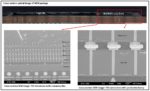
The main challenge of DRAM is bandwidth and latency. Bandwidth is the quantity of data that can be written on to the memory or can be read from it, while latency is the time gap between the request to the memory and its execution. This topic is of current interest in the memory industry. The biggest relief in bandwidth came in 2013 with the introduction of High-bandwidth-memory (HBM) where stacked DRAM dies were connected to each other by through-silicon-vias (TSV). Figure 1 shows a picture of HBM analyzed at UnitedLex in 2018 for supporting IP activities. The HBM along with its TSV structures improved the data transfer between the logic process and the memory but it did not solve the “memory wall” problem entirely.

Figure 1: Cross-section of HBM (UnitedLex)

I often wondered what the next steps would be, I then came across the proceedings of the Electronic Components and Technology Conference 2021(ECTC), which is one of the premier international events related to packaging, components, and microelectronic systems. This conference had papers from major device makers like GlobalFoundries, IBM, Intel, Micron Samsung, and TSMC. All these companies discussed hybrid bonding, direct bonding, die to die connections, and various TSV-less solutions. The one paper that caught my attention was authored by Micron Memory Japan, along with several other research organizations, and titled “Ultra-thinning of 20 nm Node DRAMS down to 3 µm for Wafer-on-Wafer (WOW) applications”. This paper describes how they thinned the wafers using two different methods namely grinding and chemical mechanical polishing (CMP) and compared retention time of the DRAM before and after the thinning. They concluded that the retention properties had not deteriorated due to the thinning process.

This was indeed a “WOW” paper. Ever since HBM was introduced, the wafer thickness has plummeted from a few hundreds of micrometers to around 40 µm but going to 3 µm is something extraordinary. Just in comparison, the human hair is around 70 µm ±20 µm. The combination of hybrid bonding and wafer thinning opens new possibilities for DRAM. In hybrid bonding the metallic bond pads of two wafers are directly connected as well as the dielectric materials adjacent to them which are also connected. Hybrid bonding is used in the industry and has been employed by Sony in their image sensors, however, as of today it has not yet been implemented in stacked DRAM products. One of the challenges of hybrid bonding is that it requires a clean interface at an atomic plane level.

The production of thin wafers along with hybrid bonding would greatly reduce the TSV impedance, it would also increase data bandwidth, reduce thermal resistance, and finally increase the density of interconnects. If such a technique were to be used then the image on figure one would not have the conductive bumps seen between the dies and the memory die thickness would be ten times thinner, which would lead to a considerable overall reduction of the height of the stack. This combination of ultra-thin wafers with hybrid bonding will extend the life of DRAM devices more easily than adopting a completely new configuration like monolithic 3D DRAM which is being lately discussed in the scientific community. New applications, like using a DRAM stack directly bonded onto a logic chip could be envisaged, or it could be used as the cache memory, like AMD and some others are implementing with their external SRAM memory. Of course, for DRAM devices, some architecture designs would need to be modified because as of today, SRAM is better than DRAM in terms of latency. Mounting thin DRAM dies on logic dies could also bring new concepts like compute in memory, where the base die in HBM could have some computing power.

DRAM devices are far from being at the end of their lives and still have many miles to go. It will need to be further shrunk to reduce costs. Probably in the future, the periphery circuitry will also be scaled or even taken out of the DRAM die and be fabricated as an independent chip and then be mounted on the DRAM using ultra thinning process and hybrid bonding technology. The combination of advanced lithography and patterning, the possibility of disaggregating periphery circuitry into individual small chips (or “chiplet”) configuration, the availability of wafer thinning process and hybrid bonding technology has rejuvenated the DRAM devices. Most likely DRAM is not ceding its place to any other memory soon. I am also hoping that there will be a breakthrough in design and process technology so that monolithic DRAM with 4F2 cell layout will be available in the market soon.

At UnitedLex, we monitor and analyze both the technology and patents that surround the IC eco-system. By doing this, we are well positioned to help clients track the innovations being implemented in industry but also, strategically guide clients on how to optimize their patent portfolios.


Auto Shows Return in Spite of COVID

Auto Shows Return in Spite of COVID
by Roger C. Lanctot on 09-26-2021 at 6:00 am

Auto Shows Return in Spite of COVID

I knew something special was going on in Munich last week at IAA Mobility – the first international auto show to be held outside China since the start of the pandemic – when a senior executive stepped off the stage before his talk to a modest crowd to say to me (sitting in the second row): “What are you doing here?” I don’t remember whether it was “What are YOU doing here?” or if it was “What are you doing HERE?” Or maybe it was “What are YOU doing HERE?”

It was a good question, but not for the reason you might think. It was logical for this European executive to be mildly surprised at the presence of an American in the middle of a European auto show in the midst of a pandemic characterized by widespread travel restrictions. It was even more surprising, though, to see ME at any auto show since I am no car enthusiast.

I was not alone. I ran into U.S. executives from Argo, Qualcomm, Intel, Lumotive, Luminar, Volkswagen, NNG, and a host of journalists and industry analysts. So, not so shocking for me to be in attendance.

There is a bizarre irony that auto shows are touted as showing off the latest technologies – giving consumers (for whom they are really intended) a taste of what the future of automotive technology holds. The reality is that entering the cockpit of a vehicle at an auto show is like entering a time machine transporting the individual back 3-4 years to what designers planned and implemented many years ago. (An exception to this are so-called “concept” cars.)

Car makers are hopelessly and routinely behind the times. It took years for car makers to accommodate smartphones and it has taken two decades for them to build in wireless connections.

Auto shows are probably the last place to go to catch a glimpse of what lies along the road ahead in automotive design. This is why IAA Mobility was so unique. Unlike its predecessor IAA (in Frankfurt), IAA Mobility included supplier companies – large and small – on the show floor and in the speeches and panel discussions.

IAA, like NAIAS, like the Geneva Motor Show, or Paris’ erstwhile Mondial de L’automobile typically feature moshpit-style press conferences, boilerplate press releases, and sterile in-booth displays. It has historically been nearly impossible at these events to have a substantive conversation regarding technical or regulatory challenges facing the industry or even user experience issues.

Traditional auto shows are all about glitz and glamour and heavy metal. This is why events such as the L.A. Auto Show’s AutomobilityLA – coming up this November – and the Future Networked Car event put on by the International Telecommunications Union in connection with the hopefully-soon-to-be-revived Geneva Show are so important. These “side shows” provide a forum to network and discuss the critical transportation issues of the day – while consumers kick the tires on the hypercars (and daily drivers) on the show floor.

The question remains: What was I doing in Munich at a car show? IAA Mobility was a car show that wasn’t a car show. That’s why I was there as were so many others.

In spite of chip shortages and related factory shutdowns, vehicle launches continue apace. New EVs are arriving nearly every week. The automotive industry is advancing and evolving and consumer demand for vehicles has never been stronger, driving up average retail prices as the reality of a scarce supply settles in.

Car companies are uniquely challenged in returning to the auto show stage as many car makers have yet to re-open their offices. Yet the new models keep coming and there is an industry-wide urge to get the word out to consumers and get the vehicles out and in front of the public.

New features and functions need to be demonstrated and explained. I went on an EV test drive recently and the initial orientation made clear that this new generation of electrified vehicles are about more than just regenerative braking and finding the right charging station.

Drivers are accessing their cars with their smartphones and accessing their infotainment systems with their Gmail credentials. The march of Google/Android-infused cars has only just begun and thus far includes the Polestar 2, Volvo XC-40, Renault Megane E-Tech, and General Motors’ Hummer EV. And the battle for the EV pickup market is gaining steam with the arrival of Ford’s Lightning F-150 and Rivian’s R1T. (Musk’s Cybertruck is delayed until late 2022.)

There is also a need to connect and interact with colleagues at auto shows. The first opportunity to do this in the U.S. will arrive at the L.A. Auto Show in November. I’ll be there, thanks to AutomobilityLA. I hope to see you there as well.

https://automobilityla.com/register/

https://laautoshow.com/tickets/


Podcast EP39: The History of TSMC with Dr. Walden Rhines

Podcast EP39: The History of TSMC with Dr. Walden Rhines
by Daniel Nenni on 09-24-2021 at 10:00 am

Dan is joined by Dr. Walden Rhines for a far-reaching discussion of the history of TSMC and the foundry business model. The past, present and potential future scenarios are all explored.

https://en.wikipedia.org/wiki/Wally_Rhines

The views, thoughts, and opinions expressed in these podcasts belong solely to the speaker, and not to the speaker’s employer, organization, committee or any other group or individual.


CEO Interview: Maxim Ershov of Diakopto

CEO Interview: Maxim Ershov of Diakopto
by Daniel Nenni on 09-24-2021 at 4:00 am

Maxim Ershov

Maxim is a scientist, engineer, and entrepreneur. His expertise is in physics, mathematics, semiconductor devices, and EDA. Prior to co-founding Diakopto, Maxim worked at Apple’s SEG (Silicon Engineering Group), where he was responsible for parasitic extraction. Before Apple, he was CTO of Silicon Frontline Technology, where he architected and successfully brought to market several industry-leading tools such as R3D and Rmap. Maxim also worked as device engineer at PDF Solutions, T-RAM Semiconductor and Foveon. Prior to moving to the industry, he was a professor at Georgia State University and University of Aizu. Maxim graduated with a Ph.D. in Solid State Electronics from the Moscow Institute of Physics and Technology, and won the first place in the Physics Olympiads (USSR) for high schools and for universities.

Tell us about what Diakopto does and what prompted you to start the company.

Diakopto was founded to help chip designers, layout engineers and CAD teams solve IC problems caused by interconnects and layout parasitics. I saw first-hand the increasing pain and headaches that parasitics were causing, delaying tapeouts by weeks or months. It was agonizing for me to watch some of the smartest engineers attempting to solve parasitics-related IC problems using a manual, trial-and-error approach that was extremely tedious and time-consuming since none of the existing tools or methodologies were helping them find where the problems were, and what was causing them. They were largely shooting in the dark, trying different things to see if the problems went away. Or they would brute-force overdesign their chips to overcome these problems, which led to higher power, area and cost.

We wanted to equip these engineers with a flashlight and a magnifying glass, to give them insight and visibility into the parasitic effects and help them find the proverbial needle in a haystack. It was for this reason that we started Diakopto and why our first tool, ParagonX, became so successful so quickly.

Where does the name Diakopto come from and why did you pick it for your company?

It’s a twist on the word “Diakoptics” which was introduced by Gabriel Kron as a method for breaking a problem down into sub-problems which can be solved independently before being joined back together to obtain an exact solution to the whole problem. We take a very similar approach in our software and methodology to solve a very large problem by slicing it into smaller sub-problems to solve.

Diakopto is also the name of a beach-front vacation town in Greece (although I have not personally had the chance to visit).

Why has parasitics become such an important factor now? What changed?

A few factors have made parasitics the increasingly dominant challenge for engineers:

The main one is the industry transition to advanced technology nodes. In FinFET technologies, the number, magnitude and impact of parasitics on chip performance, power and reliability have grown exponentially. This not only considerably slows down simulations using existing tools (often taking many days to more than a week to complete), but if the simulations reveal problems, trying to debug the problems and find out which few parasitic elements (out of thousands, millions or billions) are causing the problems is a nightmare. This is where our tools and methodology come into play – to quickly and easily pinpoint the few parasitics that need to be fixed.

We also have many customers using our products and methodology in older technologies, such as 28nm, 40nm, 90nm, even 180nm. These customers are continually pushing the envelope of these older nodes in terms of speed, accuracy, linearity, etc. This moves their designs closer and closer to the edge of the cliff of those process nodes, where parasitics suddenly become critical.

Who are your competitors? What are the differences between Diakopto’s tools and other tools?

We believe that the shift from transistor-dominated designs (pre-FinFET) to parasitics-dominated designs has driven the urgent need for a new class of tools and methodology, developed from the ground up to analyze, visualize, debug and optimize parasitic effects in modern ICs. We have opened up a new market that is mostly untapped at this time.

We complement (and do not compete with) the major signoff tools such as SPICE simulators or IR/EM tools.

There are a couple of tools that claim to help with parasitics analysis, but they are not as versatile, fast or easy to use as ParagonX. Those tools will tell you there are problems, but they do not quickly and intuitively point to the root causes.

One of the big advantages of ParagonX is the ease-of-use and out-of-the-box experience it offers: there is no need for any setup or configuration, CAD support or foundry qualification. A novice user can start using the tool after a 10 minute training, which has been unheard of in the EDA industry until now. This is why it’s easy for our tool to proliferate to new design teams, layout engineers, and CAD groups.

Diakopto seems to have come out of nowhere, but already with over 30 companies using your debugging platform. What’s the backstory?

When we first introduced our ParagonX tool in 2018, we were pleasantly overwhelmed by the high level of interest from our early customers. And very quickly, the word spread to other engineers and other companies and we have more and more customers evaluating and signing up. We are pleased to see customers using ParagonX for different foundries, process nodes, design styles, and design applications: SerDes, image sensors, data converters, PLLs, memories, low-power IoT, AR/VR, wireless/RF and many more.

Again, having a tool that is designed for unparalleled ease-of-use and that requires virtually no training or support enables a rapid adoption of ParagonX across a broad section of the industry. Once our customers validated that this is indeed the case, we felt comfortable that we could broaden our reach to the thousands of semiconductor design teams out there that we have not yet tapped into and without compromising the user experience.

Where do you see Diakopto going from here?

We are very excited about our future. Not only have we seen the adoption of ParagonX grow exponentially over the last couple of years, we are also seeing a significant uptick in the frequency and expansion of use at our customer base. Many customers have embraced and made ParagonX part of their standard flow and methodology for IC design and debugging. We have a healthy pipeline of companies currently evaluating ParagonX and we believe they will soon join our global community of customers.

We are equally encouraged by the strong tailwinds that will continue to fuel our growth. There are several key market trends that driving the increasing need for our solutions:

  • Hyperscale data centers
  • 5G wireless
  • AI/ML
  • IoT and sensors
  • AR/VR
  • Autonomous vehicles

These market trends are in turn driving the need for (1) higher speed circuits, (2) higher precision circuits, and (3) broad industry migration to advanced process technologies – all 3 of which lead to the exponentially increasing severity of parasitic effects on chip PPA and time-to-market.

What makes me even more enthusiastic is the new products that we are bringing to market to address adjacent opportunities while staying rooted in our founding principles. We will be announcing some of the new products over the coming 12 months.

Also Read:

CEO Interview: Gireesh Rajendran CEO of Steradian Semiconductors

CEO Interview: Tim Ramsdale of Agile Analog

CEO Interview: Veerbhan Kheterpal of Quadric.io


The Path to 200 Gbps Serial Links

The Path to 200 Gbps Serial Links
by Kalar Rajendiran on 09-23-2021 at 10:00 am

Industry is Quickly Scaling

Ethernet speed evolution has kept a nice pace over the years even without any competing communications standard. And there are no signs of that slowing down, thanks to innovative companies deploying creative design techniques to keep delivering high-performance SerDes IP solutions. SerDes plays an integral role in implementing highspeed Ethernet connectivity.

The voracious appetite for high-speed data connectivity is driven by applications such as 5G, 4K on-demand video, audio streaming, photo sharing, IoT and AI deep learning. The hyperscale data centers supporting many of these applications and the “enterprise move to the cloud” initiatives play catalyzing roles in driving rapid adoption of the latest SerDes technologies in implementing Ethernet solutions. 112Gbps SerDes milestone was reached just in the recent past enabling easier implementations of 400G and 800G Ethernet connections.

Last month, at the DesignCon 2021 conference, Alphawave IP made a presentation titled “The Path to 200 Gbps Serial Links.” The presentation was authored by Tony Pialis (CEO) and Clint Walker (VP Marketing) and the talk  given by Clint. Many of you know and/or have heard of Alphawave IP. They have been making waves recently in the wake of their IPO in a short span of  four years from inception of the company. According to Dealogic, this is the largest semiconductor IPO in history.

What you may not know is that Tony is a serial entrepreneur, having founded three successful companies in the highspeed connectivity space. It is hard to believe that we were discussing 5Gbps not that long ago when I first met him and he is talking 224Gbps now. Okay, it was 15 years ago during his Snowbush days when I first met him. When most other solutions at that time were taking the all-analog route, Tony was talking DSP-based implementation. He was and still appears to be a firm believer in the scalability of that approach and the results speak for themselves. One of the many products that Alphawave IP offers is a 112Gbps Long-Reach (LR), low-power, DSP-based Multi-Standard-SerDes.

Knowing Tony, Alphawave IP doesn’t rest on its laurels. Right on the heels of launching their 112Gbps SerDes, they were off to the races, experimenting in their labs to achieve 224Gbps SerDes. The presentation at the DesignCon2021 was about their experimentation, their findings and predictions based on that. This blog will summarize the key points from that presentation.

Industry Adoption of Latest Connectivity Solutions

From a data center perspective, a move toward higher speed Ethernet connectivity promises not only power savings but also area savings thereby increasing interconnect densities. So, the industry is always eager to quickly adopt technologies that will help them move in that direction.

The above figure is loaded with useful information. The middle chart is very interesting to take a closer look. When a 200Gbps SerDes becomes available, 1.6TbE becomes possible. One with an 800GbE connectivity current offering can double their connectivity speed without changing the complexity of their design too much. Alternatively, they can maintain the 800GbE connectivity offering and reduce the complexity of their design. Either way, they get to enjoy the benefits of lower power of the next gen SerDes.

Challenge of Scaling to 224Gbps SerDes

Designs adopted PAM4 signaling to support data rates beyond 25Gb/s. But PAM4 signaling is much more sensitive to noise, reflections, non-linearities and baseline wander. Receiver design is much more complicated. Refer to figure below to see the stringent requirements on signal-to-noise (SNR) ratio and jitter spec to deliver 224Gbps SerDes. In order to drive reasonable  channel lengths, insertion losses from packaging, board and cable need to be reduced in half.

Alphawave IP’s Experimentation

This presentation focuses on signal modulation experimentation to determine signaling scheme that will deliver 224Gbps rates. Alphawave IP considered 2-PAM, 4-PAM, 6-PAM, 8-PAM QPSK and 16-QAM modulation schemes for their experimentation. Higher modulation schemes introduce higher bit error rates (BER). In order to reduce BER to an acceptable 10-6 they had to improve SNR by 1-3dB. They tried advanced DSP detection to  leverage Maximum Likelihood Sequence Detectors (MLSD) in achieving 1-3dB improvement in SNR. They were able to improve BER by two orders of magnitude.

After narrowing down their choices to PAM4 and PAM6 modulation schemes, they ran experiments with two different channels per modulation scheme.

As you see in the figure above, both the channels with the PAM6 modulation scheme delivered results that meet or exceed the requirements stated earlier. BER in the 10-6 range (or better) and SNR higher than 20.5. The PAM4 modulation scheme did not deliver.

Alphawave IP’s Findings

Alphawave IP’s conclusion is that PAM6 is a feasible modulation scheme for 224Gbps long-reach electrical transmission for channels used in this study. PAM4 will work for very short reach (VSR), medium reach (MR), chip to chip (C2C) and chip to module (C2M) electrical links. A total link solution that enables PAM4 for long reach channels is preferred.

If the industry as a whole can find a way to make PAM4 possible for a total link solution, that would be a big benefit for everyone involved. This calls for collaboration among different players within the ecosystem. For example, packaging, board and cable vendors working together with the goal of reducing insertion losses to enable longer channels. System vendors working toward reducing channel length requirements.

If the industry collaborative efforts don’t yield a total link solution at PAM4, PAM6 can be used to support channels where insertion loss deteriorates too rapidly.

Summary

If you’re part of the ecosystem involved with designing and deploying high-speed connectivity solutions, you would want to discuss more details with Alphawave IP.

Also Read:

Enabling Next Generation Silicon In Package Products

Alphawave IP is Enabling 224Gbps Serial Links with DSP

CEO Interview: Tony Pialis of Alphawave IP


More Tales from the NoC Trenches

More Tales from the NoC Trenches
by Bernard Murphy on 09-23-2021 at 6:00 am

Galileo min

Science texts like to present the evolution of knowledge as step-function transitions, from ignorance to wisdom. We used to think the sun revolved around the earth. Then Galileo appeared, and we instantly realized that the earth revolves around the sun. But reality is always messier, as Galileo understood all too well. The transition from darkness to light is often bumpy. The same can be said for adopting new technologies. There may be mechanical challenges along the way, but the biggest barriers are often our own preconceptions. I talked to William Tseng (AE Manager) and Kurt Shuler (VP Marketing) at Arteris IP to share more tales from the trenches on this learning curve in NoC adoption.

Let’s go for the state-of-the-art solution!

You’re ready to make a major change in implementation architecture, so you might as well go the whole way, right? Read the latest papers, find out where all the excitement is and go for that. No compromises. According to William, this is an especially common viewpoint in research institutes. Those big organizations around the world bridge academia and industry, helping translate research ideas into something closer to real applications.

These outfits are stuffed with intellectual heavyweights, all PhDs and all well connected with counterparts in universities across the world. In their domains, they reign supreme. Not the kind of people with whom you want to get into a technical argument. Except that, like all of us, they sometimes can have a blinkered view of larger needs. Take NoCs as an example. The hot architecture is meshes because that’s what’s taking over new server and AI training SoCs. What an endorsement, right?

The bleeding edge isn’t always the right solution

This is a great direction to go if you’re building Gravitons or TPUs. Lots of uniform processors arrayed inside a mesh. But the great majority of us are building more heterogeneous systems. Containing video pipelines, roots of trust, a variety of IO peripherals, sensor fusion, inference engines, wireless connectivity. A kitchen sink of IP and connectivity needs. As an exercise, you could make that all fit inside a mesh. Distort the mesh here and there to fit larger IPs or make off-grid connections. It’s possible, but you start to wonder if it’s worth the effort. You still must meet PPA goals, and your previous design looks nothing like a mesh.

Which is where those research heavyweights start to come around. For most commercial applications, a more flexible NoC architecture is preferable. Something that can flow between IPs, as you’d expect from a NoC. That will support a mesh where an array solution is what you need but is equally at home and efficient in managing your kitchen sink of IPs and connectivity.

Use cases, architecture, and the interconnect

A challenge for any component vendor is that prospective buyers are happy to talk about the component but see no need to discuss their larger objectives. Why should software architects or product application engineers get involved in the discussion? They’ll reveal secrets the vendor shouldn’t know. Or perhaps sometimes that the integrators themselves don’t know.

William said that a common problem in helping small system teams transition to large systems is understanding how they want to manage traffic on the on-chip network. Designing effective traffic management requires some understanding of use cases. If the integrators are new to NoCs, they’ll have to turn to the NoC experts (here, Arteris IP) in a discussion together with the software and application experts. Which paths will be used most heavily? Do they know which paths must have low latency? Which can afford to be a little slower? System architects know how to answer these questions. Based on which the NoC experts can suggest an architecture for the interconnect. Architects may refine their answers over time, but once the integrators understand the NoC design concepts, they can adapt easily enough.

Coming to terms with safety

Teams with a background in small designs and now on a fast ramp are often inexperienced in all the complexities of meeting safety needs for automotive and other domains. This is another area where a component mindset can get in the way. William tells me what these kinds of integrators are looking for is an assurance that the component will be safe no matter how they use it.

Which, of course, no one can give. That’s why ISO 26262 details concepts like development interface agreements, system elements analyzed out of context and assumptions of use. Those define the boundaries around which the component vendor will provide assurances of safety.

Kurt has told me before that getting past this point takes a discussion (maybe a few). About Arteris IP experience in working with many customers in the field. About their long-standing involvement with the standard and commitment to the spirit and not just the letter of the standard. And about the practicalities of ensuring safety through the value chain, from IP to device, to module to car. Requiring not just good components but also experienced support throughout. Ultimately setting a higher bar for safety compliance than a simple checklist.

Different yes, but also better

Galileo had the harder sales job, but ultimately, he was right. People needed to change their perspectives to understand why his model was better. As they sometimes need to with NoCs. With a different perspective comes a better outcome. You can learn more about Arteris IP solutions HERE.

Also Read:

Smoothing the Path to NoC Adoption

The Zen of Auto Safety – a Path to Enlightenment

IP-XACT Resurgence, Design Enterprise Catching Up


Webinar: PICMG COM-HPC® – New Open Standard for High Performance Compute Modules

Webinar: PICMG COM-HPC® – New Open Standard for High Performance Compute Modules
by Mike Gianfagna on 09-22-2021 at 10:00 am

Webinar PICMG COM HPC® New Open Standard for High Performance Compute Modules

The subject of this webinar is focused on the new COM-HPC standard from PICMG, a nonprofit consortium of companies and organizations that collaboratively develop open standards for high performance telecommunications, military, industrial, and general-purpose embedded computing applications. A computer-on-module (COM) is a type of single-board computer that is a subtype of an embedded computer system. An extension of the concept of system on chip (SoC) and system in package (SiP), COM lies between a full-up computer and a microcontroller. These systems form a backbone for many embedded applications and the new COM-HPC® standard replaces the popular COM Express® standard, deployed in 2005. Everything is now faster and denser, so this new standard is important. Read on to learn about the new open standard for high performance compute modules.

The webinar is hosted by Mouser Electronics and Samtec. Matt Burns, technical marketing manager at Samtec is the presenter. I’ve known Matt for a long time, and I can tell you he is very knowledgeable about Samtec’s products and their impact on system design. Over the course of the last 20 years Matt has been a leader in design, technical sales and marketing in the telecommunications, medical and electronic components industries. So, what’s important about the new COM-HPC standard and why should you care? The webinar answers these questions with great clarity and depth. Let’s take a look at what you’ll learn if you attend. A replay link is coming.

Client Carrier with COM HPC module for PICMG

Spoiler alert:  The demands of PCIe 5.0 drove a lot of this. The infusion of AI into everything has also increased the need for performance. Interoperability is also front-and-center, as is the importance of edge computing. Matt explores all of these system drivers and more during the webinar. The capabilities supported by COM-HPC are discussed in detail, along with the physical channel capabilities offered by Samtec. The webinar will give you a good understanding of the hardware options available from Samtec and how they will help your system design. You can learn more about Samtec through the various posts about them on SemiWiki here.

A comparison of COM-HPC and COM Express is very helpful to understand the relative performance delivered by each of these standards. The various COM-HPC form factors are also reviewed, along with capabilities and potential applications. The COM-HPC form factors reviewed during the webinar include:

  • Size A
    • 95mm x 120mm
  • Size B
    • 120mm x 120mm
  • Size C
    • 160mm x 120mm
  • Size D
    • 160mm x 160mm
  • Size E
    • 200mmx160mm
COM HPC boards

The various client module sizes are reviewed, along with a list of possible applications. These include:

  • Medical equipment
  • High end instrumentation
  • Industrial equipment
  • Casino gaming equipment
  • Ruggedized field PCs
  • Transportation
  • Defense systems
  • AI and machine learning
  • Autonomous vehicles
  • Medical equipment
  • Cell tower base stations
  • Defense systems

Power budgets for various applications are also discussed. Some of the details of Samtec COM-HPC interconnect solutions are reviewed, including:

  • High-performance, flexible open-pin-field array
  • High-speed PCIe® 5.0 and 100 Gb Ethernet capable
  • 400 pin BGA mount
  • 4 rows x 100 columns
  • 2 / 2.4 / 2.2 mm row pitch
  • 635 mm pitch
  • 5 mm or 10 mm stack heights
  • Dimensions: 68.62 mm x 9 mm x stack height
  • Up to 360 W at 11.4 – 12.6 Volts
Samtec solutions

Details of the signal integrity performance of various Samtec solutions are also discussed, along with detailed performance plots. There is an excellent live Q&A session with the audience following the presentation for about 10 minutes. Overall, you will learn a lot during this webinar that is directly applicable to your next design project.  You can access the webinar replay here to learn about the new open standard for high performance compute modules.

Related Blog


Cautions In Using High-NA EUV

Cautions In Using High-NA EUV
by Fred Chen on 09-22-2021 at 6:00 am

Cautions In Using High NA EUV

High-NA EUV has received a lot of attention ever since Intel put the spotlight on its receiving the first 0.55 NA EUV tool from ASML [1], expected in 2025. EUV itself has numerous issues which have been enumerated by myself and others, most notoriously the stochastic defects issue. There are also a host of issues related to the propagation of the EUV light in 3D through the mask topology, with shadowing being the easiest description of the phenomenon [2]. It has already been disclosed by one EDA vendor, in fact, that EUV is being practiced with multipatterning [3], defeating the purpose for which it was originally intended. So, with the entry of high-NA EUV, the prospect of single patterning EUV makes it a very attractive option. What changes can we expect with a high-NA EUV system compared to the current EUV system?

Improvements with High-NA

The high-NA increases the numerical aperture (NA) from the current value of 0.33 to 0.55. The first benefit is this decreases the minimum optical spot size to 60% of its current value. The nominal value is given by the Rayleigh criterion of 0.61*nominal wavelength(=13.5 nm)/NA, which is 25 nm for 0.33 NA and 15 nm for 0.55 NA. This of course, helps gives a sharper aerial image, i.e., the classically projected image at the focused point in space. In reality, the image is noisier due to the limited number of photons and blurred by electrons and chemical species in the resist.

A second benefit from the high-NA system is the increased demagnification in the Y-direction (from 4X to 8X). This has the effect of reducing the spread of angles. Keeping the original 4X would have resulted in a prohibitive range of angles. This helps reduce the impact of the 3D propagation through the mask mentioned earlier. Furthermore, since the X-demagnification is the same, there is also a reduction in the range of azimuthal rotation of the plane of incidence through the slit. The illumination sine ratio (kx/4)/(ky/8) = 2 kx/ky on the mask is halved to kx/ky on the wafer, whereas for the current imaging systems the same ratio (kx/4)/(ky/4) on the mask is preserved as kx/ky on the wafer. Thus, this improves the illumination consistency through the slit.

Complications/Tradeoffs with High-NA

There are three issues with the move to a higher NA. The first should be well-known to lithographers, since it is the reduced depth of focus [4]. While the 0.33 NA 13.5 nm wavelength gives a depth of focus of 120 nm, increasing the NA to 0.55 reduces the depth of focus to a third of that, 41 nm.

The second issue is a consequence of the 8x Y-demagnification. Since the EUV mask 104 mm x 132 mm field size is not changing, the scanned field on the wafer has to be halved (in Y) from 26 mm x 33 mm to 26 mm x 16.5 mm. If a chip pattern originally took up over half the 26 mm x 33 mm field (as usually the case, even as 3 x 3 dies, for example), it would be chopped midway, leading to the need to stitch the two parts together through the exposure of two masks. Hence, double exposure patterning may creep in, spoiling the single patterning scenario.

The third issue is definitely a gotcha, since it was supposed to have been avoided at all costs in previous lithography system designs. The use of larger mirrors in the high-NA EUV system has led to unavoidable obscuration, where one mirror cannot avoiding blocking another. This has fundamental optical consequences, particularly reduction of modulation at lower spatial frequencies [5]. In some cases, the effects can be very drastic. In the example of a staggered 40 nm x 40 nm array below, the (1,1) diffraction orders is obstructed by the central obscuration in the pupil of the 0.55 NA system.

In this example, it would lead to a doubling of the spatial frequency in the x and y directions, which is a basic imaging error. Since a portion of the pupil is covered by forbidden illumination zones (shown in red), this is difficult to integrate with other patterns which normally require more flexible illumination. This is something the high-NA EUV user has to be especially aware of.

No, stochastics will not go away

The use of higher NA reduces the spot size, and hence, the image pixel size is also effectively reduced. We also expect the resist blur to be reduced in order to take advantage of higher resolution. Hence, at the same dose and k1 (feature size normalized to wavelength/NA), the number of photons in the same number of edge pixels will continue to decrease. This means the stochastic issues of EUV imaging will persist at the feature edge.

References

[1] https://www.anandtech.com/show/16823/intel-accelerated-offensive-process-roadmap-updates-to-10nm-7nm-4nm-3nm-20a-18a-packaging-foundry-emib-foveros

[2] A. Erdmann et al., “3D mask effects in high NA EUV imaging,” Proc. SPIE 10957, 109570Z (2019).

[3] https://www.ednasia.com/multi-patterning-strategies-for-navigating-the-sub-5-nm-frontier-part-3/

[4] B. J. Lin, “The k3 coefficient in nonparaxial l/NA scaling equations for resolution, depth of focus, and immersion lithography” J. Micro/Nanolith. MEMS MOEMS 1(1) 7–12 (April 2002).

[5] S. T. Yang et al., “Effect of central obscuration on image formation in projection lithography,” Proc. SPIE 1264, 477 (1990).

This article originally appeared in LinkedIn Pulse: Cautions in Using High-NA EUV

Related Lithography Posts


Arm Shifts Up With SOAFEE

Arm Shifts Up With SOAFEE
by Bernard Murphy on 09-21-2021 at 6:00 am

SOAFEE min

We’re always hearing about shift-left, advances enabling system designers to start various aspects of their development and validation earlier. In support of this goal for automotive developers, Arm recently announced their Scalable Open Architecture for Embedded Edge (SOAFEE). SOAFEE is a software platform (with reference hardware) designed to enable shift left through cloud-native software development in the new and evolving automotive world. Supporting the likes of Volkswagen who have a publicly stated goal to develop 60% of their software in-house by 2025.

Motivation

It’s no secret that automotive OEMs and others are exploring new ways to deliver and monetize mobility, as EV opportunities expand, dealership models are in question, Mobility as a Service is a hot topic and ADAS/autonomy continues to advance. Cloud service providers and others also see opportunities to claim a part of the action, seeing a move away from traditional supply chains to more collaborative development and support. Several invited Arm to drive an open architecture standard to rationalize a foundation for this software development. The standard, represented by a SIG, now includes AWS, Continental, Cariad (a VW Group company), Woven Planet (a subsidiary of Toyota), RedHat and GreenHills among others.

Why do I say Arm has shifted up to this objective? Because they are doing something they have always done well (now stretching further), which I’m now starting to see among a handful of other tech companies. Shifting up from a space in which they’ve proven themselves, to bridge a gap to the system-level needs of their ultimate system customers.

The SOAFEE Framework

SOAFEE is about enabling the software defined future of automotive. Enabling functions and capabilities through software control. Abstracting the underlying hardware to ensure portability, while preserving awareness of hardware capabilities and constraints. Putting this in place in the cloud enables OEMs to start development sooner. With that cloud-native starting point they can easily update and manage software throughout the product life cycle. Experienced cloud-based developers and app builders will also be able to contribute. All can leverage cloud-based development and deployment techniques.

Cloud-based developers still need to model realistic real-time and power behaviors. To that end, Arm has partnered with ADLINK to provide two hardware reference platforms. A 32-core Ampere Altra SoC for lab development/prototyping. And an 80-core Ampere Altra SoC in a ruggedized box for in-vehicle testing. (This box also hosts an on-board ASIL-D safety MCU.)

The software stack mirrors between the in-vehicle platform and the cloud platform. To ensure that what you develop early in the cloud should just drop into the vehicle. The same should be true for updates. Hardware and software stacks are built on top of Project Cassini (another open standard from Arm). Two major components here of interest to hardware developers are the SystemReady standard, covering a range of system compliance topics, most notably in-system PCIe compliance. And PSA-certified, covering security requirements.

Availability

The SOAFEE reference software stack is already available. The reference hardware is available for pre-order now from ADLINK.

I’m impressed. In a diverse ecosystem like the one already growing around evolving automotive needs, someone needed to step up. To ensure a common based reference for all those potential developers. Arm not only stepped up but also shifted up. To build that bridge from their world to the world in which auto solution builders want to work. You can read the press release HERE.


WEBINAR: SkillCAD now supports advanced nodes!

WEBINAR: SkillCAD now supports advanced nodes!
by Daniel Nenni on 09-20-2021 at 10:00 am

SkillCAD SemiWiki Webinar

Originally containing a handful of commands to help with common layout tasks, SkillCAD has evolved into the industry standard for analog, RF and mixed signal design for customers using Cadence Virtuoso.  With over 85 customers worldwide and over 120 functions including the powerful, patented V-editor, metal routing and pin placement tools, SkillCAD’s offering is proven to significantly improve layout design team productivity.

Today, design teams face a new challenge as the adoption of leading-edge process nodes is accelerating faster than previously anticipated due to substantial power, performance and density improvements.  The downside is that design teams are now faced with the exponential increase in design rules and time-consuming iterations of layout to achieve a “clean” design.   Project schedules suffer as layout times increase to 2X or 3X what they were in previous nodes.

The SkillCAD strength is the ability to quickly develop new layout commands that significantly improve design team productivity by automating repetitive tasks which also reduces design errors.  SkillCAD develops these new layout commands by working closely with customers who specify the functionality needed for their designs. Once the new command is developed and tested, SkillCAD then offers these new commands to all customers to be used inside the Cadence Virtuoso environment.

Today SkillCAD has over 30 commands that work with 7nm, 5nm, and 3nm. The new coloring functions are compatible with the Virtuoso coloring method, but also supports in-house coloring methods that allow designers to use a different layer purpose for different colors to minimize mouse clicks while significantly reducing the time in color editing. The new SkillCAD routing functions intelligently take advantage of the strict design rules in advanced nodes, consolidating steps into a single mouse click that can significantly increase wiring speed. SkillCAD will continue to add functionality working closely with customers to develop new commands specific to supporting advanced nodes and unique design styles.

WEBINAR REPLAY: Automating FinFET Layout

Abstract: To address the layout challenges in advanced node designs, SkillCAD has released a new module to handle the complexities associated with color-aware physical design and routing to improve the productivity of your layout team.

The new functionality offers a variety of layout capabilities for coloring and routing. The coloring functions are compatible with the Virtuoso coloring method, but also supports in-house coloring methods that allow designers to use different layer purpose for different colors to minimize mouse clicks while significantly reducing the time in color editing.

Our new routing functions intelligently take advantage of the strict design rules in advanced nodes consolidating steps into a single mouse click that can significantly increase wiring speed. SkillCAD will continue to add functionality to this new module as we work closely with our customers to develop new commands specific to advanced nodes.

Speaker: Pengwei Qian (SkillCAD)

Speaker Bio: Pengwei Qian is the founder and CEO of SkillCAD, a grassroots EDA company that has 80+ companies using IC (LAS) worldwide. Pengwei has a Bachelor’s degree in Physics and a Masters in Material Science from Fudan University and a Masters in Electronic Engineering from National University of Singapore. He started as an IC designer and now has more than 20 years of experience in EDA.

WEBINAR REPLAY: Automating FinFET Layout

About SkillCAD
Founded in 2007 to enhance productivity to Cadence Virtuoso layout design flow. Cadence Virtuoso + SkillCad have become the industry standard layout environment for full custom analog, RF, and mixed-signal designs. Over 80% of the major analog and mixed signal (AMS) companies use SkillCad. SkillCad seamlessly integrates with Cadence Virtuoso Layout L, XL and GXL and supports IC5, IC6, IC12, IC18. SkillCad has been a Cadence Connection Partner since 2008.

Also Read:

Webinar: Increase Layout Team Productivity with SkillCAD

SkillCAD Adds Powerful Editing Commands to Virtuoso

SkillCAD Layout Automation Suite has Over 120 Commands Backed by 60 Customers