RVN! 26 Banner revised (800 x 100 px) (600 x 100 px)

Webinar: Investing in Semiconductor Startups

Webinar: Investing in Semiconductor Startups
by Mike Gianfagna on 01-14-2022 at 6:00 am

Webinar Investing in Semiconductor Startups

Investing in semiconductor startups is something Silicon Catalyst knows a lot about. During a time when venture funding for chip companies all but disappeared, this remarkable organization built a robust incubator, ecosystem, support infrastructure and funding source. Silicon Catalyst has assembled a top-notch management team and an extensive, world-class advisor network. You can learn more about this remarkable organization here. Silicon Catalyst also has a great track record for putting on compelling events with A-list participants. You can read SemiWiki coverage of their most recent event here. So, when Silicon Catalyst announces a webinar on investing in semiconductor startups, you must take notice.

Chips are Popular Again

It appears the rest of the world is now seeing what Silicon Catalyst saw all along. As stated by Silicon Catalyst:

Following a remarkable year of over 25% year on year growth, the global semiconductor industry is poised to experience strong growth in 2022. World-wide sales for this year are projected to reach in excess of $600 billion in what many are calling the golden era of semiconductors.

Chips are indeed hot again. Another interesting fact courtesy of Silicon Catalyst:

Nuvia is a great example, having taken their first round of money in April 2019 at a post-money valuation of $16 million and being acquired by Qualcomm in March of 2021 for over $1.2 billion.

Examples like this are truly remarkable. They also don’t happen every day. For every home run, there are many more failures. Understanding the trends and developing insight to spot the companies that are correctly leveraging those trends is the focus of the upcoming webinar. As usual, Silicon Catalyst has assembled an all-star cast to discuss these topics. We can all learn a lot from these folks, so I highly recommend you attend this event. More information is coming.

An All-Star Cast Weighs In

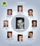
First, let’s look at the panel lineup. A stellar group from around the world.

Moderator

  • Cliff Hirsch, Semiconductor Times. Cliff has extreme depth and breadth in semiconductors and related technologies, communications, data/telecom network infrastructure, and open-source web technology. He has analyzed greater than 4,000 private and public companies in the semiconductor & comm/IT space. Check out the latest news on semiconductor startups here

Panelists

  • Rajeev Madhavan, North America, Clear Ventures. Rajeev is a founder and General Partner of Clear, where he focuses on early-stage technology investments. His notable career exits include Apigee (IPO), YuMe (IPO), Virident (acquired), Magma (IPO), Groupon (IPO), VxTel (acquired), LogicVision (IPO) and Ambit (acquired). Rajeev has the uncanny ability to deeply understand what entrepreneurs are trying to do, and to steer them onto a successful path. I know Rajeev. He truly has the golden touch.
  • Emily Meads, EU, Speed Invest. Emily passionately supports Deep Tech companies and the Deep Tech ecosystem, and always strives to give scientific credibility to the VC side of the table. Before joining Speedinvest, Emily worked for Fraunhofer IZM, as well as a software engineering startup where she first caught the startup bug. She then worked at Spin Up Science where she specifically supported innovators on their Deep Tech commercialization journeys.
  • Dov Moran, Israel: Grove Venture Capital. Dov Moran is one of Israel’s most prominent hi-tech leaders, entrepreneurs and investors. He is known as a pioneer of several flash memory technologies, most notably as the inventor of the USB flash drive. Dov was a founder and CEO of M-Systems (NSDQ: FLSH), a world leader in the flash data storage market. Under Dov’s leadership, M-Systems grew to $1B revenue, and was acquired by SanDisk Corp (NSDQ: SNDK) for $1.6B.
  • Owen Metters, UK, Foresight Williams Technology Funds. Dr. Metters is an Investment Manager at Williams Advanced Engineering (WAE). He has worked at Oxford University Innovation, the technology transfer organization for the University of Oxford, supporting academics in the commercialization of University IP leading to the formation of several successful spin-out companies which have then raised over £20m of VC funding & holds a PhD in Inorganic & Materials Chemistry from Bristol University.

And a special presentation: Semi Industry Trends and Market Opportunities for 2022, presented by:

  • Junko Yoshida, Editor in Chief, The Ojo-Yoshida Report. Junko has always been a “roving reporter” in the most literal sense. After logging 11 years of international experience at a Japanese consumer electronics company, Junko pursued journalism, breaking stories, securing exclusives, and filing incisive analyses from Tokyo, Silicon Valley, Paris, New York, and China. During her three decades at EE Times, Junko rose through the ranks from Tokyo correspondent to West Coast bureau chief, European bureau chief, news editor, and editor-in-chief.

I know Junko and I find this part quite exciting. She is someone who will always find the hidden truth in every story. Her insights are legendary. I can’t wait to hear her perspectives in her new role. She will be joined by Bolaji Ojo, Publisher and Managing Editor @The Ojo-Yoshida Report.

Junko has offered some comments about the upcoming event. Consider this a sample of what’s to come:

“Semiconductors are the lifeblood of today’s economy. It is pouring into every economic sector, at different speeds and vigor. This means there are huge investment opportunities yet to be tapped in semiconductors using new products and old ones that are finding new applications. Finding where to strategically put investment dollars in semiconductors should be a passion for every investor because this process will endure for a while. The Ojo-Yoshida Report identifies certain technology segments and market applications investors should be paying attention to.”

How to Attend the Webinar

The webinar will be held on Zoom and is open to the public. Attendees will be able to submit questions to the panel and they will be addressed as time permits.

January 19, 2022, 09:00 AM in Pacific Time (US and Canada)

You can register for the webinar on investing in semiconductor startups here.

Also Read:

Silicon Catalyst Hosts an All-Star Panel December 8th to Discuss What Happens Next?

Silicon Startups, Arm Yourself and Catalyze Your Success…. Spotlight: Semiconductor Conferences

WEBINAR: Maximizing Exit Valuations for Technology Companies


CES is Back – Partially

CES is Back – Partially
by Bill Jewell on 01-13-2022 at 2:00 pm

chart pie chart description automatically genera 2

CES (formerly the Consumer Electronics Show) returned to Las Vegas, Nevada last week. In 2021, CES was remote due to the COVID-19 pandemic. On April 28, 2021, the Consumer Technology Association (CTA), the sponsor of CES, announced CES 2022 would be held in Las Vegas. On the date of the announcement new COVID cases in the U.S. were less than 60,000 per day. On the day CES 2022 opened, January 5, 2022, new COVID cases in the U.S. were over 700,000 per day as the new omicron variant spread rapidly. Nevertheless, the show went on with COVID protocols including proof of vaccination, wearing masks indoors, social distancing, and optional on-site testing.

CTA stated CES 2022 live attendance was over 45,000 people, about a quarter of the over 175,000 attendees at the last live event, CES 2020. Over 2300 companies exhibited at CES 2022, about half the 4500 companies at CES 2020. We at Semiconductor Intelligence elected to attend CES 2022 virtually.

In conjunction with CES 2022, CTA released its forecast for U.S. consumer electronics in 2022. Total U.S. consumer electronics are projected at $293 billion, up 1.8% from 2021. Smartphones and computing are the two largest segments at about $75 billion. Video, Smart Home and Automotive are each in the $23B to $25B range.

Most categories of consumer electronics are expected to grow in the low-to mid-single-digit range in 2022. However, three emerging categories with high grow rates are virtual reality eyewear, connected exercise equipment and electric bikes.

AT CES 2022, keynote presentations were given by Samsung Electronics, General Motors, and Abbott. Interestingly only one of the three keynotes was from an electronics company.

Samsung Electronics’ keynote was led by Jong-Hee (JH) Han, Vice Chairman & CEO. The emphasis was not on products but on demonstrating commitment to the environment through a more eco-conscious product life cycle. Samsung plans to have zero standby power usage in its TVs and smartphones by 2025. Older smartphones will be repurposed for IoT applications. Samsung TVs will have solar powered remote controls to reduce battery waste.

Samsung did introduce some new products in its keynote. The Freestyle portable projector can be controlled with voice commands or wirelessly with a smartphone. It can project up to 100 inch images and includes a smart speaker. The Samsung Gaming Hub will have access to video games directly from a Samsung smart TV. The Odyssey Ark is a 55-inch gaming projector which is curved and can be aligned either horizontally or vertically. Samsung also created the home connectivity alliance (HCA) with other appliance makers to increase interoperability between products, ensure safety & data security, and increase energy efficiency.

Samsung Freestyle Projector

Samsung Odyssey Ark Monitor

General Motor’s keynote address was led by chair and CEO Mary Barra. She stated GM is transforming from an automaker to a platform innovator through electrification, software-enabled services, and autonomous driving. GM will have 30 electric vehicle (EV) models by 2025 and all new vehicle models will be electric by 2035.

GMC Hummer EV Pickup

Abott’s keynote was led by president and CEO Robert B. Ford. The keynote focused on electronic implants to improve health and health monitoring. Abbott’s Freestyle Libre glucose monitoring system uses a small sensor on the back of arm and data on a smartphone app. Its Heartmate 3 heart pump is implanted as a blood pump for people with advanced heart failure. Abbott’s neuromodulation devices alter nerve activity through electrical impulses to treat movement disorders such as Parkinson’s disease. Abbott introduced Lingo, a line of bio-wearable devices to track glucose, ketones, lactate and alcohol in order to improve diets and athletic performance.

Abbott Lingo Biosensor

Pepcom’s Digital Experience at CES 2022 introduced many innovative products as shown below.

Labrador Systems demonstrated its Labrador Retriever personal robot which can help move large loads or deliver trays. It is controlled through voice commands or a smartphone app.

Labrador Retriever

In a sign of our times, the MaskFone includes built in earphones and a microphone to enable users to talk on their smartphones in public without removing their masks.

MaskFone

Altis introduced what it claims is the world’s first artificial intelligence (AI) personal trainer. The device consists of a soundbar-sized console which uses a computer vision neural network and an exercise science deep learning model to personally instruct the user.

Altis AI Personal Trainer

Vuzix Shield smart glasses are safety classes which include video projectors, stereo sound, and noise-cancelling microphones. The Vuzix Shield glasses connect to smartphones and other devices using Wi-Fi and Bluetooth.

Vuzix Shield Smart Glasses

Hopefully CES 2023 can return to the scope of previous CES shows. Seeing in-person demonstrations of new consumer electronics is far preferable to watching videos. A live CES enables people to see, touch and even use many new devices and to talk directly to representatives of the companies. CES also brings worldwide media attention to the electronics industry.

Related Blog


It’s Now Time for Smart Clock Networks

It’s Now Time for Smart Clock Networks
by Tom Simon on 01-13-2022 at 10:00 am

Movellus Maestro Clock Network

By now most SoC designers are pretty familiar and comfortable with the use of Network on Chip (NOC) IP for interconnecting functional blocks. Looking at the underlying change that NOCs represent, we see the use of IP to supplant the use of tools for implementing a critical part of the design. The idea that ‘smart’ things are better than just structural implementation is a ubiquitous theme in our lives. Smart bulbs, smart appliances, smart thermostats, smart doorbells all make for better performance and functionality once the technology became available. The time has now come for on-chip clocking to take advantage of a smart approach through the use of IP and a new architecture to replace fixed clock trees and meshes found in previous generations of designs.

Clock networks have always been a challenging area for IC design. While they are often regarded as an unseen part of any design, they consume a significant percentage of chip power and take up considerable real estate. On top of this they are a critical factor in proper chip functionality and performance. Though for years they have been a neglected area in design flows. Movellus, a provider of clock solutions, is taking a fundamentally new approach to clock design. Instead of building a fixed clock tree out of unintelligent buffers, wires and PLLs, they use a set of intelligent IP blocks to handle the major issues encountered in clock design, skew, gating, OCV, power integrity and more.

The capabilities of the Movellus Maestro Clock Network solution is nicely summarized in a paper authored by Linley Gwennap Principal Analyst and Aakash Jani Senior Analyst with the Linley Group. The paper titled “Movellus Maestro: An Intelligent Clock

Network” explains the motivation for applying an IP based solution to clock generation and covers the benefits that result.

Historically clock networks have either been clock trees or meshes or a hybrid. Each has their own advantages and trade-offs. Clock trees tend to use less power but are subject to clock skew. Meshes reduce skew but come with an increase in power consumption. Maestro blends the two with the addition of intelligent IP that monitors skew caused by a variety of factors such as supply voltage fluctuations, OCV and temperature.

Movellus Maestro Clock Network

By virtually eliminating Skew and PVT effects higher operating frequencies can be obtained. Movellus cites some examples where usable clock periods have increased by up to 44%, allowing for much higher Fmax. Another phenomenon that Maestro manages is voltage droop when blocks are toggled on and off to conserve system power. Normally as blocks are switched on when needed there is a latency period while the power rails recover from the additional load. The Maestro Adaptive Workload Module (AWM) reduces this latency by managing clock speeds, allowing in higher system performance.

Maestro reduces the effects of OCV and power jitter on the clock by constantly monitoring and adjusting the clock network. This is especially important at near threshold voltages found in IoT devices. With proper management of OCV and jitter, margins can be reduced to improve performance and power. Maestro also employs a clever system that distributes the operation of the clock subsystems across different phases to spread out simultaneous switching IR impact from clock operation. This reduces overall power consumption and allows for improved performance.

The Linley paper covers additional details and other features of the Movellus Maestro Clock Network. It’s about time that clocks became an area for innovation. Traditionally the major players in EDA have not devoted resources to radically rethinking this crucial component of all SOCs. In a way it is surprising, given the hugely important role that clock distribution plays. The paper is available to read as a download from the Movellus website.

Also Read:

Advantages of Large-Scale Synchronous Clocking Domains in AI Chip Designs

CEO Interview: Mo Faisal of Movellus

Performance, Power and Area (PPA) Benefits Through Intelligent Clock Networks


AI at the Edge No Longer Means Dumbed-Down AI

AI at the Edge No Longer Means Dumbed-Down AI
by Bernard Murphy on 01-13-2022 at 6:00 am

face recognition

One aspect of received wisdom on AI has been that all the innovation starts in the big machine learning/training engines in the cloud. Some of that innovation might eventually migrate in a reduced/ limited form to the edge. In part this reflected the newness of the field. Perhaps also in part it reflected need for prepackaged one-size-fits-many solutions for IoT widgets. Where designers wanted the smarts in their products but weren’t quite ready to become ML design experts. But now those designers are catching up. They read the same press releases and research we all do, as do their competitors. They want to take advantage of the same advances, while sticking to power and cost constraints.

Facial Recognition

AI differentiation at the edge

It’s all about differentiation within an acceptable cost/power envelope. That’s tough to get from pre-packaged solutions. Competitors have access to the same solutions after all. What you really want is a set of algorithm options modeled in the processor as dedicated accelerators ready to be utilized, with ability to layer on your own software-based value-add. You might think there can’t be much you can do here, outside of some admin and tuning. Times have changed. CEVA recently introduced their NeuPro-M embedded AI processor which allows optimization using some of the latest ML advances, deep into algorithm design.

OK, so more control of the algorithm, but to what end? You want to optimize performance per watt, but the standard metric – TOPS/W – is too coarse. Imaging applications should be measured against frames per second (fps) per watt. For security applications, for automotive safety, or drone collision avoidance, recognition times per frame are much more relevant than raw operations per second. So a platform like NeuPro-M which can deliver up to thousands of fps/W in principle will handle realistic fps rates of 30-60 frames per second at very low power. That’s a real advance on traditional pre-packaged AI solutions.

Making it possible

Ultimate algorithms are built by dialing in the features you’ve read about, starting with a wide range of quantization options. The same applies to data type diversity in activation and weights across a range of bit-sizes. The neural multiplier unit (NMU) optimally supports multiple bit-width options for activation and weights such as 8×2 or 16×4 and will also support variants like 8×10.

The processor supports Winograd Transforms or efficient convolutions, providing up to 2X performance gain and reduced power with limited precision degradation. Add the sparsity engine to the model for up to 4X acceleration depending on quantity of zero-values (in either data or weights). Here, the Neural Multiplier Unit also supports a range of data types, fixed from 2×2 to 16×16, and floating point (and Bfloat) from 16×16 to 32×32.

Streaming logic provides options for fixed point scaling, activation and pooling. The vector processor allows you to add your own custom layers to the model. “So what, everyone supports that”, you might think but see below on throughput. There are also a set of next generation AI features including vision transformers, 3D convolution, RNN support, and matrix decomposition.

Lots of algorithm options, all supported by a network optimization to your embedded solution through the CDNN framework to fully exploit the power of your ML algorithms. CDNN is a combination of a network inferencing graph compiler and a dedicated PyTorch add-on tool. This tool will prune the model, optionally supports model compression through matrix decomposition, and adds quantization-aware re-training.

Throughput optimization

In most AI systems, some of these functions might be handled in specialized engines, requiring data to be offloaded and the transform to be loaded back when completed. That’s a lot of added latency (and maybe power compromises), completely undermining performance in your otherwise strong model. NeuPro-M eliminates that issue by connecting all these accelerators directly to a shared L1 cache. Sustaining much higher bandwidth than you’ll find in conventional accelerators.

As a striking example, the vector processing unit, typically used to define custom layers, sits at the same level as the other accelerators. Your algorithms implemented in the VPU benefit from the same acceleration as the rest of the model. Again, no offload and reload needed to accelerate custom layers. In addition, you can have up to 8 of these NPM engines (all the accelerators, plus the NPM L1 cache). NeuPro-M also offers a significant level of software-controlled bandwidth optimization between the L2 cache and the L1 caches, optimizing frame handling and minimizing need for DDR accesses.

Naturally NeuPro-M will also minimize data and weight traffic . For data, accelerators share the same L1 cache. A host processor can communicate data directly with the NeuPro-M L2, again reducing need for DDR transfers. NeuPro-M compresses and decompresses weights on-chip in transfer with DDR memory. It can do the same with activations.

The proof in fps/W acceleration

CEVA ran standard benchmarks using a combination of algorithms modeled in the accelerators, from native through Winograd, to Winograd+Sparsity, to Winograd+Sparsity+4×4. Both benchmarks showed performance improvements up to 3X, with power (fps/W) by around 5X for an ISP NN. The NeuPro-M solution delivered smaller area, a 4X performance, 1/3 of the power, compared with their earlier generation NeuPro-S.

There is a trend I am seeing more generally to get the ultimate in performance by combining multiple algorithms. Which is what CEVA has now made possible with this platform. You can read more HERE.

Also Read:

RedCap Will Accelerate 5G for IoT

Ultra-Wide Band Finds New Relevance

Low Power Positioning for Logistics – Ultimate Tracking


From Now to 2025 – Changes in Store for Hardware-Assisted Verification

From Now to 2025 – Changes in Store for Hardware-Assisted Verification
by Daniel Nenni on 01-12-2022 at 6:00 am

Jean Marie Brunet

Lauro Rizzatti recently interviewed Jean-Marie Brunet, vice president of product management and product engineering in the Scalable Verification Solution division at Siemens EDA, about why hardware-assisted verification is a must have for today’s semiconductor designs. A condensed version of their discussion is below.

LR: There were a number of hardware-assisted verification announcements in 2021. What is your take on these announcements?

JMB: Yes, 2021 was a year of major announcements in the hardware-assisted verification space.

Cadence announced a combination of emulation and prototyping focused on reducing the cost of verification by having prototyping take over tasks from the emulator when faster speed is needed.

Synopsys announced ZeBu-EP1, positioned as a fast-prototyping solution. It isn’t clear what the acronym means, but I believe it stands for enterprise prototyping. After several years of maintaining that ZeBu is the fastest emulator on the market, Synopsys launched a new hardware platform as a fast (or faster) emulator. Is it because ZeBu 4 is not fast enough? More to the point, what is the difference between ZeBu and HAPS?

In March 2021, Siemens EDA announced three new Veloce hardware platform products: Veloce Strato+, Veloce Primo and Veloce proFPGA. Each of these products addresses different verification tasks at different stages in the verification cycle. The launch answered a need for hardware-assisted verification to be a staged, progressive path toward working silicon. Customers want to verify their designs at each stage within the context of real workloads where time to results is as fast as possible without compromising the quality of testing.

In stage 1, blocks, IP and subsystems are assembled into a final SoC. At this stage, very fast compile and effective debug is needed with less emphasis on runtime.

At stage 2, the assembled SoC is becoming a full RTL description. Now, design verification requires a hardware platform that can run faster than the traditional emulator. One that needs less compilation, less debug but more runtime.

In stage 3, verification moves progressively toward system validation. Here it’s about full performance where cabling interconnect to the hardware allows it to run as fast as possible.

LR: Let’s look at the question of tool capacity. Some SoC designs exceed 10-billion gates making capacity a critical parameter for hardware platforms. A perplexing question has to do with capacity scalability. For example, does a complex, 10-billion gate design (one design) have the same requirements as 10, one-billion gate designs (multiple designs) in terms of usable emulation capacity?

JMB: This question always triggers intense discussions with our customers in the emulation and prototyping community. Let me try to explain why it’s so important. Depending on the customer, their total capacity needs may be 10-, 20- or 30-billion gates. In our conversation with customers, we then inquire about the largest design they plan to emulate. The answer depends on the platform they’re using. Today, the largest monolithic designs are in the range of 10- to 15-billion gates. For the sake of this conversation, let’s use 10-billion gates as a typical measure.

The question is, do they manage a single monolithic design of 10-billion gates in the same way they manage 10, one-billion gate designs? The two scenarios have equivalent capacity requirements, but not the same emulation complexity.

Emulating a 10-billion gate design is a complex task. The emulator must be architected to accommodate large designs from the ground up through the chip and subsystem to the system level including requirements at the software level.

A compiler that can map large designs across multiple chips, across multiple chassis is necessary. A critical issue is the architecture that drives the emulation interconnect. If not properly designed and optimized, overall performance and capacity scaling drops considerably.

With off-the-shelf FPGAs as the functioning chip on the boards, the DUT is spread across each interconnected FPGA, lowering the capacity of each FPGA. By interconnecting multiple chassis, the overall performance drops below that of one or a few FPGAs.

Synopsys positions its FPGA-based tools as the fastest emulator for designs in the ballpark of one-billion gates. The speed of the system clock is high because FPGAs are fast. When enough hardware is assembled to run 10-billion gates, an engineer ends up interconnecting large arrays of FPGAs that were never designed for this application. And typically, the interconnection network is an afterthought conceived to accommodate those arrays. This is different from a custom chip-based platform where the interconnection is designed as an integral part of the emulator.

Cadence claims support for very high capacity in the 19-billion gate range. The reality is that no customer is emulating that size of design. The key to supporting high-capacity requirements is the interconnect network. It doesn’t appear that the Palladium Z2 interconnect network is different from the network in Palladium Z1, which is known for capacity scaling issues. As a result, customers should ask if Palladium Z2 has the ability to map a 10-billion gate design reliably.

Today, Veloce Strato+ is the only hardware platform that can execute 10-billion gate designs in a monolithic structure reliably with repeatable results without suffering speed degradation.

The challenge concerns the scaling of the interconnect network. Some emulation architectures are better than others. Based on the roadmap taken by different vendors, future scaling will get even more challenging.

By 2025, the largest design sizes will be in the range of 25-billion gates or even more. If today’s engineering groups are struggling to emulate a design at 10-billion gates, how will they emulate 25 billion+ gates?

Siemens EDA is uniquely positioned to handle very large designs, reliably and at speed, and we continue to develop next-generation hardware platforms to stay ahead of the growing complexity and size of tomorrow’s designs.

LR: Besides the necessary capacity, what other attributes are required to efficiently verify complex, 10-billion gate designs?

JMB: Virtualization of the test environment is as important as capacity and performance.

In the course of the verification cycle, the DUT representation evolves from a virtual description (high level of abstraction) to a hybrid description that mixes RTL and virtual models, such as AFMs or QEMU. Eventually, it becomes a gate-level netlist. When an engineer is not testing a DUT in ICE (in circuit emulation) mode, the test environment is described at a high level of abstraction typically consisting of software workloads.

It’s been understood for a while that RTL simulation cannot keep up with execution of high-level abstraction models running on the server. The larger the high-level abstraction portion of the DUT, the faster the verification. The sooner software workloads are executed, the faster the verification cycle. This is the definition of a shift-left methodology. A virtual/hybrid/RTL representation is needed to run real software workloads on an SoC as accurately as possible and as fast as possible. An efficient verification environment allows a fast, seamless move from virtual to hybrid, from hybrid to RTL, and from RTL to gate.

The hybrid environment decouples an engineer from the performance bottleneck of full RTL, which supports much faster execution. In fact, hybrid can also support software development that is not possible in an RTL environment. A full RTL DUT runs in the emulator with very limited interaction with the server in hybrid mode or the parts of the DUT that run on the server. Here the connection between server and platform, or what we call co-model communication, becomes critical. If not architected properly, the overall performance fails to be acceptable. Unlike the bottleneck of the emulator, now the bottleneck is the communication channel.

We have invested significant engineering resources to address this bottleneck. Our environment excels in virtual/hybrid mode because of our unique co-model channel technology

Capacity, performance and virtualization are the key attributes to handle designs of 10+-billion gates. When designs hit 25 billion+ gates in 2025, the communication channel efficiency becomes even more critical since hybrid emulation becomes prevalent in a wide range of applications.

LR: Thank you, Jean-Marie, for your perspectives and for explaining some of the little-known aspects of successful hardware emulation use.

Also Read:

DAC 2021 – Taming Process Variability in Semiconductor IP

DAC 2021 – Siemens EDA talks about using the Cloud

DAC 2021 – Joe Sawicki explains Digitalization


DAC 2021 – What’s Up with Agnisys and Spec-driven IC Development

DAC 2021 – What’s Up with Agnisys and Spec-driven IC Development
by Daniel Payne on 01-11-2022 at 10:00 am

IDesignSpec min 1

Walking the exhibit floors at DAC in December I spotted the familiar face of Anupam  Bakshi, Founder and CEO of Agnisys, so I stopped by the booth to get an update on his EDA company. My first question for him was about the origin of the company name, Agnisys, and I found at that Agni means Fire in Sanskrit, one of the five elements.

Agnisys at #58DAC

The company vision is the same today as it was from the founding, it’s a tool flow going from the specification to implementation, across design and verification and SW and device drivers. Having a single source of truth on registers for all engineering groups to know and use is a core idea. IDesignSpec is their EDA tool launched 11 years ago now, and the scope of the tool has only grown over time.

IDesignSpec

There are now resellers of Agnisys tools in all continents, the number of licenses have been going up, and the new trend is for site licensing, instead of having just a handful of licenses on one project. When one IC design team starts using IDesignSpec, then other adjacent teams start to hear about the benefits and want to give it a try on their project too.

Another EDA tool at Agnisys is called ISequenceSpec, released about three years ago, and it helps engineers to capture sequences as stimulus generation used in verification, firmware and even post-silicon validation. ISequenceSpec can convert into UVM or C levels. Here’s where ISequenceSpec fits into a design flow:

ISequenceSpec

The newest EDA tool has taken a totally different approach to introduction, because it is being crowd-sourced, and it’s called ISpec.ai. What’s unique is that this tool automatically converts English assertions into proper SystemVerilog Assertions (SVA) by using Machine Learning (ML) techniques. So the company finds out what engineers think about when learning SVA, and then the users can give Yes (Green) or No (Red) feedback, leaving any comments about the quality of the conversion. This tool was released about 2-3 months ago, then existing customers became aware of it and started testing, and so far about 200 engineers have provided feedback.

iSpec.ai

They have even offered quizzes to see if engineers can answer questions about SVA with or without using iSpec.ai, which is kind of fun and technical at the same time. So this tool in a way is kind of similar to Google Translate, as it translates in both directions, both into SVA or English. The company plans to productize this web-based tool after a learning phase.

DVCon US 2022 is coming up in February, and Agnisys has a paper on the iSpec.ai tool, so consider attending that online event to see what progress has been made so far.

Co-located with DAC this year was the RISC-V conference, and Agnisys presented on, “A System Level Verification and Validation Environment using SweRV”. You can watch this 10 minute presentation on YouTube, and it was a Lightning Talk. SweRV is an open-source RISC-V core from Western Digital.

RISC-V Lightning Talk

Connecting all of the semiconductor IPs together in a system-level environment, your team either does this by hand or with some automation. Using SweRV as the processor you can then connect together tests at the IP or system level. Using the C to UVM interface, then both levels can talk together. The processor knows C, while the other IPs understand UVM. So you can run your C program, and it then causes UVM transactions by the tool using SweRV.

Another new tool in 2021 is called IDS-FPGA, now part of the IDesignSpec family, so that FPGA design teams can reduce their development times by using an approach with automated code generation, IP generators, and have an integrated flow with FPGA vendor software. They support the Xilinx UltraScale+ IP-based design development, and have integration with Xilinx Vivado and the Intel Quartus Prime architectures.

Summary

Agnisys has a 15 year history in providing their IDesignSpec tool, and it just keeps getting more robust each year. This company is one of the very few EDA vendors that actually demonstrates their tool live, running on a laptop, so it wasn’t just a PowerPoint presentation at DAC. I think that engineers are really attracted to seeing an EDA tool running live, because they are curious at how the GUI looks, how quickly it operates, and how intuitive the flow is.

Also read:

AI for EDA for AI

What the Heck is Collaborative Specification?

AUGER, the First User Group Meeting for Agnisys


Horizontal, Vertical, and Slanted Line Shadowing Across Slit in Low-NA and High-NA EUV Lithography Systems

Horizontal, Vertical, and Slanted Line Shadowing Across Slit in Low-NA and High-NA EUV Lithography Systems
by Fred Chen on 01-11-2022 at 6:00 am

EUV shadowing across slit

EUV lithography systems continue to be the source of much hope for continuing the pace of increasing device density on wafers per Moore’s Law. Recently, although EUV systems were originally supposed to help the industry avoid much multipatterning, it has not turned out to be the case [1,2]. The main surprise has been the rise of stochastic defects and variability [1,2], which challenge both dose and overlay control. It has constrained sub-20 nm features to be printed with multipatterning assistance such as SALELE [3]. This has also accelerated the development of the next-generation High-NA EUV tools [4,5] in order to bring back the opportunity for avoiding multipatterning. On the other hand, High-NA tools have their own concerns as well [4-6].

EUV technology requires a substantially different infrastructure from previous optical lithography. A fundamental reason is it is based on reflective optics rather than transmissive optics. Even the mask needs to be built on a reflective multilayer substrate. This, in turn, has led to some distinct quirks in the EUV imaging process. Due to the reflection being an inherently off-axis process, the illumination of the mask has some inherent asymmetry, as shown in Figure 1[7].

Figure 1. EUV illumination of the mask is essentially a rotated off-axis angle across an arc-shaped slit. Illustration is based from Figure 1 in [7].

There is an arc-shaped slit, 26 mm across and ~1-2 mm thick (depending on design), through which a central illumination ray angle of 6 degrees is rotated azimuthally. As a result, features in the center of the exposure field are actually illuminated at different angles from features at the edge of the exposure field. Each different angle produces a different effective “shadow” which comprehends the light’s propagation through and reflection by the multilayer substrate, as well as double pass through the mask pattern [8]. Such shadowing could cause loss of image contrast (also known as fading) [9].

Figure 2. A particular illumination at the slit center is rotated at the slit edge. Illustration is based from Figure 9 in [10].

Consequently, the horizontal vs vertical line shadowing behavior varies across slit. The appropriate metric for the degree of shadowing is the larger incident angle, at the mask, in the direction perpendicular to the lines between the two pole angles in an ideal dipole illumination setup (targeting sine=0.5 wavelength/pitch at the wafer) for the slit center. Some results are shown in Figure 3 for horizontal and vertical lines. Low-NA (NA=0.33) and High-NA (NA=0.55) systems are plotted side by side.

Figure 3. Horizontal and vertical line shadowing vs slit position, for different pitches on both 0.33 and 0.55 NA systems.

There are several things to point out.

  1. In all cases, the smaller pitch has worse shadowing, i.e., a larger incident angle for one of the illumination poles compared to the other.
  2. The vertical line shadowing varies linearly across slit, because when the azimuthal angle flips sign going from one side of the slit to the other, light is still shining on one side of the line but casts a growing or diminishing shadow.
  3. The horizontal line shadowing is worse than the vertical line shadowing.
  4. High-NA tools do not necessarily provide relief from shadowing, particularly for vertical lines, at pitches targeted for High-NA.
  5. The doubling of demagnification in the High-NA tools from 4x to 8x causes equal shadowing at half the pitch for the latter.

DRAM active areas (Figure 4) present an interesting special case, for they are neither horizontal nor vertical but slanted in between.

Figure 4. Shadowing for DRAM active area lines (angled at 14.5 degrees with respect to the horizontal).  

As may be expected, the shadowing for slanted lines has combined characteristics of horizontal and vertical lines. The High-NA tool does not necessarily provide less shadowing than the Low-NA tool, but the range of shadowing across slit is less. Low-NA tools already show significant shadowing for 16-nm half-pitch, while High-NA tools do so for 10-nm half-pitch.

References

[1] https://m.blog.naver.com/PostView.naver?blogId=jkhan012&logNo=222410469787&categoryNo=30&proxyReferer=https:%2F%2Fwww.linkedin.com%2F

[2] D. De Simone and G. Vandenberghe, “Printability study of EUV double patterning for CMOS metal layers,” Proc. SPIE 10957, 109570Q (2019).

[3] K. Sah et al., “Defect characterization of EUV Self-Aligned Litho-Etch Litho-Etch (SALELE) patterning scheme for advanced nodes,” Proc. SPIE 11611, 116112H (2021).

[4] E. van Setten et al., “High NA EUV lithography: Next step in EUV imaging,” Proc. SPIE 10957, 1095709 (2019).

[5] https://www.imec-int.com/en/articles/high-na-euvl-next-major-step-lithography

[6] A. H. Gabor et al., “Effect of high NA “half-field” printing on overlay error,” Proc. SPIE 11609, 1160907 (2021).

[7] P. C. W. Ng et al., “A Fully Model-Based Methodology for Simultaneously Correcting EUV Mask Shadowing and Optical Proximity Effects with Improved Pattern Transfer Fidelity and Process Windows,” Proc. SPIE 7520, 75200S (2009).

[8] E. van Setten et al., “Multilayer optimization for high-NA EUV mask3D suppression,” Proc. SPIE 11517, 115170Y (2020).

[9] C. van Lare, F. Timmermans, and J. Finders, “Mask-absorber optimization: the next phase,” J. Micro/Nanolith. MEMS MOEMS 19, 024401 (2020).

[10] H. Tanabe, “Classification of EUV masks based on the ratio of the complex refractive index k/(1-n),” Proc. SPIE 11854, 11581416 (2021).

This article originally appeared in LinkedIn Pulse: Horizontal, Vertical , and Slanted Line Shadowing Across Slit in Low-NA and High-NA EUV Lithography Systems


Can you Simulate me now? Ansys and Keysight Prototype in 5G

Can you Simulate me now? Ansys and Keysight Prototype in 5G
by Shawn Carpenter on 01-10-2022 at 10:00 am

5G Signal propagation

Ansys and Keysight wanted to see if they could answer the question, If we put virtual cellphones in different locations in a city, can we predict what kind of 5G signal we’re going to get in those locations? To find out, they created and tested a detailed virtual model of a city, including a variety of 5G antennae, receivers, and transmitters typically found in a high-density urban area. It turns out, we can.

The team used Ansys HFSS to construct 5G MIMO base station antenna array models and handset antenna models for a 28 GHz, high-band system and placed them in different locations around a realistic city model. From there, they used HFSS SBR+ to figure out what was really happening between the antennas by using physics to model the propagation of signals between the base station and the handsets.

5G Signal propagation through complex city environments is modeled with a Shooting and Bouncing Rays (SBR) electromagnetic field solver. These signal propagation simulations are linked to detailed Ansys HFSS phased array base station and handset antenna system models.

Together, Ansys and Keysight tested a proof of concept for an accurate, physics-based virtualized process for understanding 5G physical channel behavior. The prototype was a true partnership between Ansys and Keysight capabilities. Ansys methodology was leveraged to model the physical layer—virtual antennas, scattering, and their coupling tendencies—on top of Keysight’s method for modeling the actual 5G radio architecture and beam selection process.

Ansys HFSS and HFSS SBR+ are used to compute the physical channel response for an installed 5G base station array and user equipment antennas, and Keysight SystemVue extracts the time domain channel properties, recreating user signal angle of arrival for MIMO beamforming.

Eventually, virtual modeling will take the place of the “hunt and peck” method of installing and adjusting 5G base stations to maximize coverage. For detailed information on the proof of concept, check out our recent webinar, 5G mm-wave Physical Channel Modeling with EM Physics.

What problems can we solve with 5G virtual modeling?

5G promises mid-band and high-band channels capable of delivering massive quantities of data at blindingly fast speeds. 5G radio equipment vendors and wireless service providers quote impressive capabilities for high-band systems at 28 and 39 GHz. The catch is: these systems are only cost effective in high-population areas, like city centers.

There are four main factors that complicate 5G systems beyond what we were seeing at lower-band frequencies:

More Drops
At high frequencies, the farther away from the base station, the more signals are dropped. The speed of drop off is about ten times faster in 5G. A highly populated area requires many more access points to service all subscribers.

Low Signal Penetration
Signals have a hard time penetrating common building materials at high bands in the mm-wave frequencies. A 4G mobile phone inside a building can receive signal from a cellular tower miles away because these lower frequency longer wavelength signals can penetrate the structures and surfaces between the phone and the tower. At the higher frequency 5G bands, buildings go from acting like signal sponges to acting like mirrors. At 28GHz, a popular 5G high band frequency, plate glass (1.5-centimeter thickness) reduces signal penetration by a factor of one thousand. Physically thicker cement and brick pose even worse attenuation. The mirror effect of exterior surfaces creates another problem: delay spread. With signals bouncing everywhere, receivers get delayed copies of the signal, making receiver design much more complicated.

Distance Loss
5G systems operate using antennas that concentrate signal energy in spot beams to overcome the signal distance losses that increase more quickly than in 4G. It’s critical to identify the right locations for access points such that every subscriber is covered with minimal overlap. It’s possible to test real-world installations and locations, but it’s time consuming and expensive. High-frequency, high-bandwidth measurement equipment is considerably more expensive, even cost prohibitive at times.

Bureaucratic Delay

Getting a permit from a city council or other governing body to install a 5G antenna system can be an arduous process. Nobody wants to get approved for 10 mount locations and find out that 5 of them are non-optimal, so they need to go back to the drawing board and re-apply with the city. The key is to identify the right number of access points, in the right locations, to offer consistent coverage with the fewest number of access points possible.

All of these issues can be solved with a virtualized process. Can we let the computer show us how well we’re serving a city’s subscribers? Ansys and Keysight say yes.

Animation of the E-fields of a 28 GHz signal with 400 MHz bandwidth traveling from a phased array base station model into a city environment. The signal bounces off the street (bottom) and the wall of a facing building (right). Single frequency electric field is shown in the top left for 2 cut planes.

What does the future of the electronics industry look like?

The short answer: partnerships. After many years of competing, Ansys and Keysight see more ways to move the industry forward by working as a complementary pair.

“Between Ansys and our partners, we stand a chance at creating the first digital twin of a 5G network that can cooperate with an actual, living network,” said Shawn Carpenter, Program Director 5G & Space at Ansys.

Using the existing prototype, Ansys and Keysight can tell you what signals are transmitted and received, but it’s much harder to address the five or six network layers that might be involved when a subscriber pulls out their smart phone to use a navigational app. How do we identify the shortest route across the network to the Cloud? How do we get data to the Cloud while maintaining data integrity? What delays do we expect in getting data our handset requests?

Many of the data communications issues are simply outside Ansys HFSS’ purview. The environment we use for our electromagnetics modeling is fantastic for modeling antenna systems or radio frequency components, but it’s not designed to model complete cities with interconnected cars driving up and down the streets, drones flying through it, and aircraft flying over the top.

In 2020, Ansys acquired Analytical Graphics Incorporated (AGI), a specialist in multi-domain mission engineering. AGI has incredible capabilities that extend into the 5G space too. This prototype included a few subscribers, but the real world is a lot more dense, and AGI’s know-how will assist in evaluating complex networks and simulating at scale. AGI also partners with Scalable Network Technologies, a master at answering these kinds of questions. Just recently, Scalable Networks was acquired by Keysight. To entangle the knot even further, AGI already has an existing interface for their network modeling tools inside of Keysight’s STK Interface. Between Ansys, Keysight, AGI, Scalable Network Technologies, and our other complementary partners, we have what we need to simulate and emulate at scale, and we’ll continue to polish our workflow integration.

Also Read

Cut Out the Cutouts

Is Ansys Reviving the Collaborative Business Model in EDA?

A Practical Approach to Better Thermal Analysis for Chip and Package


IBM at IEDM

IBM at IEDM
by Scotten Jones on 01-10-2022 at 6:00 am

Vertical FET process

IBM transferred their semiconductor manufacturing to GLOBALFOUNDRIES several years ago but still maintains a multibillion-dollar research facility at Albany Nanotech. IBM is very active at conferences such as IEDM and appears to have a good public relations department because they get a lot of press.

At the Litho Workshop in 2019 I heard an IBM presentation from the Albany research group, explaining that IBM had to have the research line because they needed state-of-the-art technology for the processors that run their computers. I personally question this rational, the Albany Research group collaborated with Samsung on the 5nm process Samsung put into production. I estimate that Samsung’s 5nm process when compared to TSMC’s 5nm process – has 1.69x the power consumption (worse), 0.64x the performance (worse), and 0.72x the density (worse). I am sure there are special features in the process to support IBM, but I am also sure the same features could be implemented in the TSMC process without a multibillion-dollar research investment. I also thought it was interesting that they said that while developing the process they turned up the EUV dose until they got good yield and then they transferred it to Samsung expecting Samsung to reduce the EUV dose. When Samsung began ramping their 5nm process there were industry rumors Samsung couldn’t get enough wafers through their EUV tools (high EUV dose leads to low throughput) and the yields were low.

IBM also makes a big splash in the mainstream press every few years with some new development but in my opinion a lot of the developments don’t live up to the hype. For example, in early 2021 IBM announced the development of a 2nm technology but as I have previously written it is more like TSMC’s 3nm process that 2nm, and unlikely to be competitive versus expected 2nm processes from Intel and TSMC. You can read my 2nm article here: https://semiwiki.com/semiconductor-services/ic-knowledge/298875-is-ibms-2nm-announcement-actually-a-2nm-node/

This is not to say that IBM doesn’t do important research, years ago they were responsible for many key industry innovations including copper metallization, I just question whether a multibillion-dollar semiconductor research facility makes sense for a company that doesn’t make semiconductors.

In this article I will discuss three IBM papers from IEDM.

Vertical-Transport Nanosheet Technology for CMOS Scaling beyond Lateral-Transport Devices

In my opinion this paper is another example of an IBM announcement I don’t expect to live up to the hype. Authors note, this work was done in cooperation with Samsung. The mainstream media has already published about this “breakthrough” as if it will be a production solution.

Figure 1 illustrates the Vertical-Transport Nanosheet (VTFET) process.

Figure 1. Vertical-Transport Nanosheet (VTFET) process.

The basic idea here is to make nanosheets but rather than in the horizontal direction, to turn them into the vertical direction. In the paper a vertical nanosheet is compared to a FinFET and shown to offer better performance and area. I see two issues with this.

First, my understanding is vertical transistors are very favorable for SRAM usage where the interconnect needs are simple and regular but doesn’t work well for random logic designs with complex interconnect needs.  Imec has previously shown some very interesting vertical SRAM work although it doesn’t appear to have gained any traction in the industry. With the advent of chiplets a simple SRAM process that offers superior density makes a lot of sense. But once again, for logic use the vertical transistor area would likely go up a lot to accommodate the interconnect requirements.

The second issue I see with this is it is being compared to FinFETs. The transitions away from FinFETs to stacked horizontal nanosheets (HNS) is already under way. HNS offers density and performance advantages over FinFETs, but even more importantly offers a long-term scaling path. HNS can improve performance by stacking more sheets vertically, they also open the opportunity to introduce a dielectric wall creating an Imec innovation called Forksheets with reduced n to p spacing. Beyond this, stacking n and p HNS in a 3D-CMOS/CFET architecture offers more scaling with zero horizontal n to p spacing. Beyond HNS, the sheets can potentially be replaced with 2D materials providing even more scaling. Drive current and therefore performance of vertical fins is driven by the fin size, and I don’t see how the devices can scale the way HNS can. I believe this is why the industry has chosen HNS as the successor to FinFETs, Samsung is already trying to ramp a HNS process (Samsung calls it Multibridge), Intel is planning HNS (Intel calls them RibbonFETs) for 2024 and TSMC has published HNS work and is widely expected to adopt them for 2nm (although they haven’t formally announced their 2nm process technology selection).

Critical Elements for Next Generation High Performance Computing Nanosheet Technology

In my view this paper is a lot more interesting than the previous one because it is addressing issues with the HNS technology that all the major leading edge logic suppliers are facing. IBM has done a lot of good work on HNS in the past and this paper builds on that.

There are two HNS issues addressed in this paper.

The first issue is that pFET mobility is poor for HNS. IBM has previously described two techniques to improve pFET mobility, one is to trim back the channel after release and deposit a SiGe cladding layer. Another technique is fabricating the channels on a strain relaxed buffer layer.

In this paper SiGe channels were formed by depositing lower Ge content channels over higher Ge content sacrificial layers when the original nanosheet stack is deposited. The difference in Ge content is to enable the selective release etch, to etch out the sacrificial films and leave the channels intact. The SiGe channel provides improved mobility, improved performance, and greater reliability.

Figure 2 illustrates the SiGe channel HNS pFET.

Figure 2. SiGe channel HNS pFET.

The second issue addressed here is how to achieve multiple-uniform threshold voltages (Vts) for HNS. For FinFETs the fin-to-fin distance is relatively wide and multiple Vts can be achieved by depositing and selectively removing multiple work function metals. With HNS the sheet to sheet (Tsus) spacing is so small that there isn’t enough space for a full stack of work function metals. The metals also tend to be thicker on the outside of the NS and thinner in between the nano sheets leading to non-uniform Vts.

IBM pioneered the use of dipoles to control VT over decade ago and that technique is now getting a lot of attention for HNS because dipoles can be created by doping the high-k dielectric and don’t require extra thickness the way multiple work function metals do. Dipoles can also fix the Vt non uniformity issue.

Figure 3 illustrates how work function metals can lead to non-uniform Vts and how volumeless dipoles fix the problem.

Figure 3. Work Function metal versus Dipoles for Vt control. (a) Pure metal multi-Vt scheme which could cause huge Vt non-uniformity for high nVt device and high pVt device and (b) Volumeless multi-Vt reduces nWFM thickness and share the metals to improve the Vt uniformity.

Gate-Last I/O Transistors based on Stacked Gate-All-Around Nanosheet Architecture for Advanced Logic Technologies

The third paper I wanted to discuss is another paper looking at HNS issues.

Another challenge in HNS implementation is how to create I/O transistors that can operate at higher voltage. In this paper a gate last process flow creates two different gate oxide thicknesses with a combination of deposited oxide and novel selective oxidation. The selective oxidation creates thick and thin selective oxides that are added to the deposited oxide. The key to this technique is that grown oxide consumes silicon during oxidation and therefore the thicker grown oxide consumes more silicon than the thin grown oxide opening up the sheet to sheet spacing (Tsus) to accommodate the thicker oxide.

Figure 4 illustrates thick and thin gated oxide HNS devices and the improved Tsus to accommodate the thick oxide.

Figure 4.- Thick and thin gate oxide HNS devices with increased Tsus for the thick I/O oxide devices.

Conclusion

Despite the mainstream media hype about IBM’s Vertical-Transport Nanosheet announcement at IEDM, we believe it is IBM’s work on perfecting HNS processes is more likely to have an impact on the industry. pFET channel mobility, volume less Vt solutions and high voltage I/O solutions address problems the industry is currently wrestling with for the FinFET to HNS transition

Related Blog


Your Smart Device Will Feel Your Pain & Fear

Your Smart Device Will Feel Your Pain & Fear
by admin on 01-09-2022 at 6:00 am

Your Smart Device Will Feel Your Pain Fear

What if your smart device could empathize with you? The evolving field known as affective computing is likely to make it happen soon. Scientists and engineers are developing systems and devices that can recognize, interpret, process, and simulate human affects or emotions. It is an interdisciplinary field spanning computer science, psychology, and cognitive science. While its origins can be traced to longstanding philosophical inquiries into emotion, a 1995 paper on #affective computing by Rosalind Picard catalyzed modern progress.

The more smart devices we have in our lives, the more we are going to want them to behave politely and be socially smart. We don’t want them to bother us with unimportant information or overload us with too much information. That kind of common-sense reasoning requires an understanding of our emotional state. We’re starting to see such systems perform specific, predefined functions, like changing in real time how you are presented with the questions in a quiz, or recommending a set of videos in an educational program to fit the changing mood of students.

How can we make a device that responds appropriately to your emotional state? Researchers are using sensors, microphones, and cameras combined with software logic. A device with the ability to detect and appropriately respond to a user’s emotions and other stimuli could gather cues from a variety of sources. Facial expressions, posture, gestures, speech, the force or rhythm of key strokes, and the temperature changes of a hand on a mouse can all potentially signify emotional changes that can be detected and interpreted by a computer. A built-in camera, for example, may capture images of a user. Speech, gesture, and facial recognition technologies are being explored for affective computing applications.

Just looking at speech alone, a computer can observe innumerable variables that may indicate emotional reaction and variation. Among these are a person’s rate of speaking, accent, pitch, pitch range, final lowering, stress frequency, breathlessness, brilliance, loudness, and discontinuities in the pattern of pauses or pitch.

Gestures can also be used to detect emotional states, especially when used in conjunction with speech and face recognition. Such gestures might include simple reflexive responses, like lifting your shoulders when you don’t know the answer to a question. Or they could be complex and meaningful, as when communicating with sign language.

A third approach is the monitoring of physiological signs. These might include pulse and heart rate or minute contractions of facial muscles. Pulses in blood volume can be monitored, as can what’s known as galvanic skin response. This area of research is still in relative new but it is gaining momentum and we are starting to see real products that implement the techniques.

Source: galvanic skin response, Explorer Research

Recognizing emotional information requires the extraction of meaningful patterns from the gathered data. Some researchers are using machine learning techniques to detect such patterns.

Detecting emotion in people is one thing. But work is also going into computers that themselves show what appear to be emotions. Already in use are systems that simulate emotions in automated telephone and online conversation agents to facilitate interactivity between human and machine.

There are many applications for affective computing. One is in education. Such systems can help address one of the major drawbacks of online learning versus in-classroom learning: the difficulty faced by teachers in adapting pedagogical situations to the emotional state of students in the classroom. In e-learning applications, affective computing can adjust the presentation style of a computerized tutor when a learner is bored, interested, frustrated, or pleased. Psychological health services also benefit from affective computing applications that can determine a client’s emotional state.

Robotic systems capable of processing affective information can offer more functionality alongside human workers in uncertain or complex environments. Companion devices, such as digital pets, can use affective computing abilities to enhance realism and display a higher degree of autonomy.

Other potential applications can be found in social monitoring. For example, a car might monitor the emotion of all occupants and invoke additional safety measures, potentially alerting other vehicles if it detects the driver to be angry. Affective computing has potential applications in human-computer interaction, such as affective “mirrors” that allow the user to see how he or she performs. One example might be warning signals that tell a driver if they are sleepy or going too fast or too slow. A system might even call relatives if the driver is sick or drunk (though one can imagine mixed reactions on the part of the driver to such developments). Emotion-monitoring agents might issue a warning before one sends an angry email, or a music player could select tracks based on your mood. Companies may even be able to use affective computing to infer whether their products will be well-received by the market by detecting facial or speech changes in potential customers when they read an ad or first use the product. Affective computing is also starting to be applied to the development of communicative technologies for use by people with autism.

Many universities done extensive work on affective computing resulting projects include something called the galvactivator which was a good starting point. It’s a glove-like wearable device that senses a wearer’s skin conductivity and maps values to a bright LED display. Increases in skin conductivity across the palm tend to indicate physiological arousal, so the display glows brightly. This may have many potentially useful purposes, including self-feedback for stress management, facilitation of conversation between two people, or visualizing aspects of attention while learning. Along with the revolution in wearable computing technology, affective computing is poised to become more widely accepted, and there will be endless applications for affective computing in many aspects of life.

One of the future applications will be the use of affective computing in #Metaverse applications, which will humanize the avatar and add emotion as 5th dimension opening limitless possibilities, but all these advancements in applications of affective computing racing to make the machines more human will come with challenges namely SSP (Security, Safety, Privacy) the three pillars of online user, we need to make sure all the three pillars of online user are protected and well defined , it’s easier said than done but clear guidelines of what , where, who, who will use the data will make acceptance of hardware and software of affective computing faster without replacing physical pain with mental pain of fear of privacy and security and safety of our data .

References

https://www.linkedin.com/pulse/20140424221437-246665791-affective-computing/

https://www.linkedin.com/pulse/20140730042327-246665791-your-computer-will-feel-your-pain/