RVN! 26 Banner revised (800 x 100 px) (600 x 100 px)

KLAC- Great quarter and year – March Q is turning point of supply chain problem

KLAC- Great quarter and year – March Q is turning point of supply chain problem
by Robert Maire on 01-30-2022 at 10:00 am

KLAC Foundry Logic

-KLAC – great QTR & calendar year but supply chain impacted
-Management feels supply chain to improve after March Q
-Demand remains strong, driven by foundry/logic
-Process management is next best place in industry after litho

Great end to calendar year

KLA reported revenues of $2.53B with non GAAP EPS of $5.59 nicely exceeding street expectation of $2.33B and EPS of $5.45. Guidance was muted due to supply chain issues at $2.2B +-$100M and Non GAAP EPS of $4.80+-$0.45. This is versus expectations of $2.37B and $5.50 in EPS

March is worst of supply chain impact

Management was clear and adamant that March would be the worst of the supply chain impact and that things would improve going forward for the remainder of the year . The company estimated that the March quarter would see an 8-10% negative impact on revenue. Importantly that revenue would likely ship in June creating the uptick.

This is certainly in contrast to Lam that didn’t identify a clear end to their issues and seemed to be more open ended as to how long there would be supply chain issues. While we are certainly not happy to see the issues finally crop up we feel better that the impact seems to be for one quarter with most all the revenue just slipping into the next quarter.

In KLA’s case, there is essentially zero likelihood that KLA will lose any revenue to competitors as they supply very unique products and are certainly less interchangeable as compared to dep and etch products.

Process control continues to outperform overall WFE

Process control tools such as those made by KLA continue to grow faster than the overall market as rapidly increasing process complexity requires more process control at higher costs as we continue to push the limits of physics.

Process control follows litho sales and complexity and is somewhat of a shadow proxy for ASML’s sales and growth. Wafer and especially reticle inspection are driven by the increasing lithographic challenges. We see this out performance in the mid to high single digits continuing in 2022.

Being a play on foundry helps in the current environment

While Lam remains the poster child for memory manufacturing so too does KLA remain the poster child for foundry/logic which was 79% of business.
The huge bump up in spend by TSMC coupled with what will likely be a large bump up by Intel as well, will clearly benefit KLA as those are two key and significant customers.

While memory spend remains solid it is also conservative as the industry wants to have supply and demand remain in balance. The challenges in 3D NAND are clearly one of the big drivers of process control in the memory space.

Backlog is Beautiful

KLA has historically had good backlog which enables them to dial in and control their numbers better than most in the industry. We know that some KLA products are quoting deliveries of over a year and a years backlog in products at this point given such strong demand is not out of the norm.

While KLA’s backlog may not exactly be like ASML’s its not far off. KLA obviously has the added benefit of superb gross margins. The current super strong demand environment coupled with the constrained supply chain will keep backlog high and likely growing. Although the supply chains issues may get better after the March quarter , we think backlog will remain high due to current demand which will not diminish.

The Stock

Investors will obviously not like the weak guide for the March quarter but the negative impact on the stock should be more muted as the worst of it will be March and things will pick up after that with the revenue just slipping into June.
Obviously the overall market sentiment and volatility is quite horrible so the limitation of the impact to a single quarter may not matter as investors are just in a general supply chain panic.

We could see some collateral help from Apple talking about supply chain issues improving which would lend credence to KLA’s view of March as the low point with the rest of the year up from there.

The stock has lost quite a bit for such a high quality name which makes us feel more attracted to it especially if it were to trade off too sharply.
Unfortunately the recent volatility continues to reduce predictability and makes investors wary of even high quality stories.

About Semiconductor Advisors LLC
Semiconductor Advisors is an RIA (a Registered Investment Advisor),
specializing in technology companies with particular emphasis on semiconductor and semiconductor equipment companies. We have been covering the space longer and been involved with more transactions than any other financial professional in the space. We provide research, consulting and advisory services on strategic and financial matters to both industry participants as well as investors. We offer expert, intelligent, balanced research and advice. Our opinions are very direct and honest and offer an unbiased view as compared to other sources.

Also Read:

LRCX- Supply Chain Catches up with Lam- Gets worse before better- Demand solid

ASML Too Much Demand Plus Intel and High NA

Forty Four Billion Reasons Why TSMC Remains Dominant


Apple and OnStar: Privacy vs. Emergency Response

Apple and OnStar: Privacy vs. Emergency Response
by Roger C. Lanctot on 01-30-2022 at 8:00 am

Apple and OnStar Privacy vs. Emergency Response

In the season 6 premiere of Showtime’s “Billions,”, financier Michael Prince and his lieutenant are remotely monitoring Wags’ heart rate thanks to an Oura-like smart ring as he works out on a Peloton stationary bike. The remote observers conclude Wags is having a heart attack and dispatch emergency medical technicians to his aid without his knowledge.

This kind of experience may soon become more common as a growing range of devices are enabled with connectivity and sensors to identify or anticipate emergencies ranging from heart attacks to car crashes. In fact, emergency response is becoming a theme in television advertising most recently from Apple and General Motors’ OnStar.

Apple: https://9to5mac.com/2022/01/01/apple-watch-emergency-sos-911/

OnStar: https://www.youtube.com/watch?v=jhVqHLqK4M4

The issue of automatic crash detection is front of mind in the U.S. thanks to the universal shutoff of 3G wireless service which robbed a few million cars in the U.S. of their automatic crash notification functions. This is not an issue in Europe (yet) where so-called eCall has been a mandatory automotive feature since 2018. (Europe is currently facing its own 2G/3G shutoff challenges.)

The key difference between the experience of an Apple Watch SOS user or an OnStar subscriber and the scene depicted in “Billions” is that Apple and OnStar customers must knowingly activate and/or opt-into use of the service.  Wags in “Billions,” on the other hand, is a victim of a privacy violation.

The point is, emergency response is swiftly becoming a high profile connected service. RapidSOS, a leading platform provider in this space, already has 400M SOS-equipped devices on its network representing 65 companies including SiriusXM, TrueMotion, Farmers’ Insurance, Lemonade, Apple, and Uber.

The challenge is to get the story right – helping consumers understand the value proposition and how and why it works the way it does. The two commercials in question get some things right – but the OnStar commercial gets a lot wrong.

The Apple Watch commercial gets the SOS function right because it shows that the smartwatch will dial 911 directly (via a Bluetooth connection to an iPhone or Wi-Fi) if the user doesn’t cancel the call. The OnStar commercial gets this message wrong because it portrays the OnStar operator speaking directly with the first responder on the scene.

In reality, the OnStar operator contacts the relevant emergency call center (public service access point) and provides information delivered from the car and the customer. It is also not unusual for the OnStar operator to remain on the line to continue to exchange information between the customer and the PSAP. But the call center operator usually handles the communication to the first responders on their way to or at the scene.

Inadvertently, OnStar’s commercial – which was taken off the air almost as quickly as it appeared – does demonstrate the value of communicating valuable, if not essential information directly to first responders at an emergency event. Most basic ACN systems deliver latitude and longitude information, vehicle make and model and color, some crash severity info, vehicle VIN, and time of the incident.

Time is important, because the whole point of automatic crash notification in cars is to reduce the response time by immediately determining that an event has occurred. According to published analysis of emergency response calls, each minute of response time, represents a 7% reduction in mortality (mainly for non-automotive scenarios).

This is why RapidSOS has developed a massive middleware integration infrastructure for quickly processing information from incidents and sending it on to the PSAP. RapidSOS has been successful in delivering on this value proposition and increasingly dominates the emergency response market.

RapidSOS is at the forefront of a transformation of emergency response systems. The industry is poised to revolutionize this application as the technology finds its way into smartwatches, smartphones, cars, home security systems, and any number of other personal and mobile devices – like smart rings.

The risk to the automotive industry, though, is that the introduction of crash detection into smartphones – it is already available in Google’s Pixel phones – may lead consumers to believe they don’t need it in their cars. Consumers may come to regard smartphone-based 911 in the U.S. as “good enough” ACN. What it will really amount to is ACN-lite – tastes great, less useful. (Europe has yet to allow smartphone-based ACN capability.)

First responders already need and want more information about a crash as they arrive at the scene. What is missing is the integration of off-board data such as:

  • Vehicle ownership
  • Whether the car is stolen
  • Fire and extraction protocols – if the car is an EV
  • Customer towing preference
  • Emergency contacts or next of kin
  • Existing medical conditions of driver, passengers

Having all of this information is especially important if the driver of the vehicle is unconscious. One company has emerged to integrate this essential off-board data: Roadside Telematics.

Apple and Google cannot deliver this kind of information. Properly configured ACN systems equipped with RapidSOS compatibility and linked to technology from Roadside Telematics will be able to deliver on the last-mile proposition of getting vital information to first responders at the scenes of crashes.

RapidSOS estimates that upwards of 150,000 lives could be saved for all sorts of incidents with more timely processing of event information. This is why the company integrates with a wide range of applications currently in use at emergency call centers. Getting the last mile information correct – using Roadside Telematics – will contribute to these life-saving implementations.

For organizations with devices capable of generating emergency calls – such as Apple and OnStar – it is now more important than ever to get the messaging right. Consumers need to be educated that this is one circumstance where sharing personal information may be a life-saving proposition.

Also Read:

Musk: Colossus of Roads, with Achilles’​ Heel

RedCap Will Accelerate 5G for IoT

Traceability and ISO 26262


LRCX- Supply Chain Catches up with Lam- Gets worse before better- Demand solid

LRCX- Supply Chain Catches up with Lam- Gets worse before better- Demand solid
by Robert Maire on 01-30-2022 at 6:00 am

Lam Research

-Supply chain issues finally catch up to Lam- Ongoing issue
-Problem from one main supplier to spread to more
-Causes low December Quarter and soft guide for March
-Quarters could be lumpy due to differed & revenue push outs

Lam Stews over supply Chain Issues

It sucks when you have all the demand in the world but can’t build enough product. Its even worse when the problem is getting worse before it gets better. Lam, which had previously dodged supply chain issues when Applied Materials got hit, now has its own issues.

The company reported revenues of $4.23B below street estimates of $4.4B and below conservative mid point of guidance. Earnings were more of less in line at $8.53 versus street of $8.52 and were actually light if you back out a one time investment gain. Guidance is not that great at all, at $4.25B +-$300M with EPS of $7.45 +- $0.75. This is way, way short of current estimates of $4.5B and $8.72 in EPS.

Sloppy quarters due to revenue movement

Lam suggested that the March quarter could see $500M in revenue deferrals as revenue slips out of the quarter due to supply chain issues. Product can be shipped without missing subsystems to be reunited at the customer installation site. This is similar to what we had heard from ASML who has a way more complex tool.

Situation gets worse before better

Lam suggested on the call that the issue was primarily one key supplier in the last two weeks of the quarter but that the problem was broadening to other sub suppliers.

We think the problem has likely been around for a bit longer than the last two weeks of the quarter as it was described as being at least three areas of 1) Labor, 2) Freight and 3) Supply Chain.

Perhaps its that while Lam may have hit prior issues and dealt with them, the severity of the issue probably became insurmountable.
One of the key questions that will weigh on the stock is how much worse it gets and for how long

Demand remains strong

Demand exceeds supply…..At this point anything beyond that doesn’t matter. Obviously the supply issue in the semiconductor industry remains with us and all manufacturers and would be manufacturers , like China, continue to place orders and wait in line.

Focus is entirely on fixing the supply chain

Management sounds like it is laser focused on fixing the supply chains issues. Most likely resorting to daily beatings of sub suppliers, looking for alternate suppliers and scouring the globe for needed parts inventory.
God help the sub supplier who cant ‘fix their issues or messes up.

Lam also had the unfortunate timing to be moving a lot of production to Malaysia in the middle of this supply chain crisis. We understand its likely not possible to delay the transition but it makes things just that much worse.
Margins are negatively impacted as you have the costs associated with Malaysia before you get a full ramp of production.

Concerns about market share loss

We have pointed out a number of times that we remain concerned about share loss when tool makers can’t fulfill orders. Desperate chip makers, hungry for tools might be tempted to order competitors tools that are not as good or more expensive.

Even worse, uncertainty of delivery could cause customers to double or triple order from Lam, Applied and TEL etc in hopes of taking the first tool that gets delivered.

While this is not not an issue on critical applications like “drill and pray” deep etches for NAND where Lam commands the market, it could become a problem on more generic , easy applications that are more competitive.

The Stock is gonna get trashed

LRCX was already off 5% in the after market….even though that seems like nothing in light of the recent overall market volatility. We think the stock could get very badly hit as the market is not in a positive mood and any bad news such as what Lam delivered will likely have an overreaction.

The reality is that the semiconductor equipment stocks had been overbought and have been correcting for a while anyway….this will certainly speed up the correction.

We don’t see any reason to go out and buy the stock any time soon as the uncertainty is getting worse and will keep investors waiting. We also don’t see a price at which we would be a buyer given the current momentum and tone.

As far as collateral damage goes, the other tools makers like AMAT and KLAC will likely see some sympathetic weakness in their stock. We don’t expect AMAT to buck the supply chain issue trend that they have already reported. Its more likely it has worsened.

KLAC is likely most resistant to supply chain issues but is certainly far from immune. TEL in Japan may be more secure as most of their supply chain is from inside Japan and is much tighter relationships exist in Japan.

Our two conclusions are that supply chain issues are still getting worse in some cases and are clearly longer than expected and two, that this years performance may have upside limited in growth due to these supply issues more than previously anticipated.

About Semiconductor Advisors LLC
Semiconductor Advisors is an RIA (a Registered Investment Advisor),
specializing in technology companies with particular emphasis on semiconductor and semiconductor equipment companies. We have been covering the space longer and been involved with more transactions than any other financial professional in the space. We provide research, consulting and advisory services on strategic and financial matters to both industry participants as well as investors. We offer expert, intelligent, balanced research and advice. Our opinions are very direct and honest and offer an unbiased view as compared to other sources.

Also read:

ASML Too Much Demand Plus Intel and High NA

Forty Four Billion Reasons Why TSMC Remains Dominant“Too Big To Fail Two” – Could chip failure take down tech & entire economy?

TSMC Earnings – The Handoff from Mobile to HPC


Tesla: Kick-ass Radio in an EV

Tesla: Kick-ass Radio in an EV
by Roger C. Lanctot on 01-29-2022 at 6:00 am

Tesla Kick ass Radio in an EV

It seems that all we hear about over-the-air radio broadcasts in electric vehicles is that AM is going away due to interference and FM is irrelevant due to streaming apps. Tesla has very affirmatively upended this conventional wisdom with an over-the-air update that adds Xperi’s DTS AutoStage to most Tesla’s.

This free software update, just the latest in a long string, brings metadata for station identification and artwork to the in-dash radio experience. It also reveals a lot about how in-car radio is evolving.

First of all, as is illustrated in the image (above), some stations may not have metadata associated with their displayed icon. In Tesla’s case this is most likely due to the strong radio reception in Tesla vehicles exceeding the anticipated coverage radius defined by DTS AutoStage. This is easily corrected, but a tip of the hat to Tesla’s engineers.

The display of 18 station logos also raises real questions as to how drivers will interact with the radio. The radio dial was abandoned long ago. Will we select stations by voice or touch? How will we search?

The bigger issue is that Tesla has brought this experience to dashboards with an over-the-air update with little or no fanfare. Tesla is expected to add a Radio Traffic Alert function via over the air update and will be adding Dolby Atmos audio enhancements via over-the-air update.

This is in addition to adding Emergency Safety Solution’s Hazard Enhanced Location Protocol broadcast (H.E.L.P.) functionality via over-the air update. HELP is designed to alert oncoming cars when a Tesla – or similarly equipped vehicle – is disabled along the side of the road due to a crash or breakdown.

And this, too, is in addition to Full Self-Driving having been switched on for thousands, if not hundreds of thousands, of Tesla drivers in the past few weeks. Tesla is calling the tune in the automotive industry from the standpoint of both innovation and speed to market.

We always knew that over-the-air updates would help preserve the value of so-equipped vehicles, such as Teslas. What we didn’t expect was that Tesla would become the go-to partner for industry startups seeking the fastest route to market.

Where the average auto maker offers a 2-3 year implementation plan to new market entrants. Tesla offers the prospect of instant deployment along with the ability to assess consumer response also almost instantly.

The preservation and enhancement of vehicle value has been proven as used Teslas are routinely resold at the same prices at which they were acquired. But serving as a platform for innovation means every dreamer with a new idea for safer driving or in-vehicle content consumption is making Tesla a first stop.

It so happens that in the process, radio has benefited handsomely with new content and interfaces. But, actually, if you want the state of the art in a connected radio experience you probably still have to look to Mercedes-Benz or Hyundai. Tesla’s DTS AutoState implementation uses only static station data and has not yet implemented artist and track information – already deployed in select Mercedes-Benz and Hyundai vehicles. But if you want Dolby, Tesla will be the place to look and listen.

Also Read:

Regulators Wrestle with ‘Explainability’​

Functional Safety for Automotive IP

Don’t Lie to Me


Podcast EP59: A brief history of semiconductors and EDA with Rich Goldman

Podcast EP59: A brief history of semiconductors and EDA with Rich Goldman
by Daniel Nenni on 01-28-2022 at 10:00 am

Dan is joined by good friend and fellow boater Rich Goldman. Rich has a storied career in EDA that began at TI with Morris Chang and Wally Rhines, continued through a long career at Synopsys and included a book collaboration with Neil Armstrong, Stephen Hawking and Brian May (the lead guitarist for Queen),

Dan and Rich cover a lot of ground across both semiconductors and EDA, the innovation, the trends and what it means.

Book reference: Starmus

The views, thoughts, and opinions expressed in these podcasts belong solely to the speaker, and not to the speaker’s employer, organization, committee or any other group or individual.


WEBINAR: How to add a NIST-Certified Random Number Generator to any IoT device?

WEBINAR: How to add a NIST-Certified Random Number Generator to any IoT device?
by Daniel Nenni on 01-28-2022 at 6:00 am

Intrinsic ID Webinar Blog

In the first half of 2021, the number of attacks on IoT devices more than doubled to 1.5 billion attacks in just six months. These attacks target some typical weaknesses, such as the use of weak passwords, lack of regular patches and updates, insecure interfaces, and insufficient data protection. However, researchers from Bishop Fox recently identified a new critical vulnerability of IoT devices that might not be so obvious to many of us. Their study showed that hardware random number generators (RNGs) used in billions of IoT devices fail to provide sufficient entropy. Insufficient entropy causes predictable instead of random numbers, which severely compromises the foundation of many cryptographic algorithms. Secret keys will lose their strength, leading to broken encryption.

REPLAY is HERE

So a new approach for generating random numbers is needed. This webinar shows how large amounts of entropy can be extracted from unpredictable SRAM behavior. Using this method only requires a software installation, meaning the security systems of billions of devices can be patched without the need to make hardware changes, even in devices that have already been deployed.

What will you learn?

This webinar shows how you can utilize Zign™ RNG, the Intrinsic ID embedded software IP for random number generation, to add a NIST-certified random number generator to any device, simply using software. The webinar will explain to you:

  • Why having a trusted RNG is important for any IoT device
  • How entropy can be harvested from unpredictable SRAM behavior
  • How this entropy is used to create a strong RNG
  • Which steps have been taken to turn Zign RNG into a NIST-certified RNG

Who should attend?

This webinar is must-see for anyone responsible for product design and/or embedded security of IoT chips and devices. Whether you are a semiconductor professional or an IoT device maker, this webinar will show you how you add a trusted source of strong entropy to your product without making any changes to your hardware.

About Zign RNG

Zign RNG is an embedded software IP solution from Intrinsic ID that that leverages the unpredictable behavior of existing SRAM to generate entropy in IoT devices. This approach enables anyone to add a random number generator to their products without the need for hardware modifications. The Zign RNG product is compliant with the NIST SP 800-90 standard, and it is the only hardware entropy source that does not need to be loaded at silicon fabrication. It can be installed later in the supply chain, and even retrofitted on already-deployed devices. This enables a never-before-possible “brownfield” deployment of a cryptographically secure, NIST-certified RNG.

About the Speaker: Nicolas Moro

Nicolas Moro holds a PhD in Computer Science from Université Pierre et Marie Curie in Paris. After receiving his PhD, he worked in varying R&D roles at NXP and Imec. Two years ago Nicolas joined Intrinsic ID, where he works as a Senior Embedded Software Engineer. He has extensive experience in embedded systems security and is the author of several research papers about fault injection attacks and software countermeasures.

REPLAY is HERE

About Intrinsic-ID

Intrinsic ID is the world’s leading provider of security IP for embedded systems based on PUF technology. The technology provides an additional level of hardware security utilizing the inherent uniqueness in each and every silicon chip. The IP can be delivered in hardware or software and can be applied easily to almost any chip – from tiny microcontrollers to high-performance FPGAs – and at any stage of a product’s lifecycle. It is used as a hardware root of trust to protect sensitive military and government data and systems, validate payment systems, secure connectivity, and authenticate sensors. Intrinsic ID security has been deployed and proven in hundreds of millions of devices certified by EMVCo, Visa, CC EAL6+, PSA, ioXt, and governments across the globe.

Also Read:

Enlisting Entropy to Generate Secure SoC Root Keys
Using PUFs for Random Number Generation
Quantum Computing and Threats to Secure Communication

SIP Modules Solve Numerous Scaling Problems – But Introduce New Issues

SIP Modules Solve Numerous Scaling Problems – But Introduce New Issues
by Tom Simon on 01-27-2022 at 10:00 am

SIP Verification

Multi-chip modules are now more important than ever, even though the basic concept has been around for decades. With The effects of Moore’s Law and other factors such as yield, power, and process choices, reasons for dividing what once would have been a single SOC into multiple die and integrating them in a single module have become extraordinarily compelling. These system in package (SIP) modules are becoming ever more popular. Yet for all their advantages, they do add a level of design and verification complexity that must be addressed.

SIP Verification

There are many good reasons to use SIP modules. SIP modules let designers break up large die into several smaller dies, which lessens the impact of a fabrication defect. Instead of throwing away an entire large die, only the smaller die affected by a failure need to be replaced. Also, some parts of a large system can easily be fabricated on a lower cost and less technically complex die based on a trailing process node. Similarly, memories, RF and other specialized functional units can reside on their own die using any needed process technology such as NAND memory, GaAs, etc. High speed SerDes for off-chip links can also use legacy analog nodes to save costs and reduce design risk. SIP modules also reduce PCB component counts and simplify board design.

On the flip side, these benefits come with increased complexity. They introduce a new level of interconnect that needs to be verified for correct connectivity. Substrate connections from each die need to be logically correct, and also the geometry of the connections require verification. The pad centers need to be checked for proper alignment. Device scaling and orientation are factors that can determine if the final fabricated parts are functional. Different die and elements used to construct SIP modules have unique thermal properties which can affect the integrity of the bump to pad connections. All of this calls for a solution to ensure that the design is correct.

To help design teams deal with the added complexity of SIP module verification, Siemens EDA has developed a tool called Xpedition Substrate Integrator (xSI) that provides an integrated solution for defining and consolidating all pertinent module design data, allowing for the definition of the golden design intent. There is native integration with Calibre 3DSTACK to provide robust automated DRC/LVS checking for SIP modules. Justin Locke from Siemens has authored a white paper that describes the need for a DRC/LVS specifically targeted at SIP modules. The white paper is titled “System-in-Package/Module Assembly Verification”.

There are several unique challenges that are faced by SIP module verification tools. Because it sits at the nexus between board and die, the task of verifying SIP Modules has to interface with multiple tool flows and also multiple design teams. This data and organization complexity has to be a primary focus for any tool. Additionally, during earlier stages of the flow, the full GDS may not be available to help locate and identify the pads on the die. Siemens xSI offers the ability to create dummy die information that can be used in the interim until the full GDS information if available. Once GDS for the die is available, it can be used to ensure proper pad centering and connection overlap.

System in Package is here now. Design teams need to work with them to deliver market winning products. Today’s SIP modules are a far cry from the old multi-chip modules. It comes as a relief that there are tool solutions tailored to help deliver high quality finished products. The full Siemens white paper is available for reading on the Siemens website.

Also read:

MBIST Power Creates Lurking Danger for SOCs

From Now to 2025 – Changes in Store for Hardware-Assisted Verification

DAC 2021 – Taming Process Variability in Semiconductor IP


Samsung Keynote at IEDM

Samsung Keynote at IEDM
by Scotten Jones on 01-27-2022 at 6:00 am

Samsung Keynote Figure 1

Kinam Kim is a longtime Samsung technologist who has published many excellent articles over the years. He is now the Chairman of Samsung Electronics, and he gave a very interesting keynote address at IEDM.

He began with some general observations:

The world is experiencing a transformation powered by semiconductors that has been accelerated by COVID due to lock downs requiring contactless society. IT has become essential due to remote work, and remote education. Sensors, processors, and memory are all required. Digital adoption has taken a quantum leap and 25% remote work has increased to 58%. The digitization of the economy presents tremendous opportunity, smarts systems are generating tremendous amounts of data. Over the past 50 years, transistors per wafer are up by 10 million times, processor speeds by 100 thousand times, and costs down 47% per year. Semiconductors have similarity to the human brain, sensor are like eyes, processors and memory do the processing and storing. Smart phones combining sensors with processing enable new applications, sensors are taking on a bigger role with autonomous driving, AI, etc.

There was an interesting section on sensors but that isn’t really my area and I want to focus on the logic, DRAM and NAND roadmaps he presented.

Figure 1 presents the logic roadmap.

Figure 1. Logic Roadmap.

In figure 1 we can see how the contacted poly pitch (CPP) of logic processes has scaled over time. In the planar era we saw high-k metal gate (HKMG) introduced by Intel at 45nm and by the foundries at 28nm as well as innovations like embedded silicon germanium (eSiGe) to improve channel performance through strain. FinFETs were introduced by Intel at 22nm and adopted by the foundries at 14/16nm and have carried the industry forward for several nodes. Samsung is currently trying to lead the industry into the Gate All Around (GAA) era with horizontal nanosheets (HNS) they call multi bridge and HNS should carry the industry for at least two nodes. Beyond 2nm Samsung anticipates one of either a 3D Stacked FET (called a CFET or 3D FET by others), VFET as recently disclosed by IBM and Samsung, 2D materials or a negative capacitance FET (NCFET).

Figure 2 presents the roadmap for DRAM.

Figure 2 DRAM Roadmap

With EUV already ramping up in DRAM, the next challenges are shrinking the memory cell. Samsung is anticipating staking two layers of capacitors soon. A switch to vertical access transistor is anticipated in the later part of the decade followed by 3D DRAM. I haven’t been able to find much specific information on how 3D DRAM will be built but similar structures are illustrated in presentations from ASM, Applied Materials and Tokyo Electron as well as this presentation making it appear that the industry is converging on a solution.

Figure 3 presents the roadmap for NAND.

Figure 3 NAND Roadmap

Samsung’s latest 3D NAND is a 176-layer process that uses string stacking for the first time (first time string stacking for them, others have been string stacking for multiple generations) and peripheral under the array for the first time (once again the first time for them, others have been doing it for several generations). Next up is shrinking the spacing between the channel holes to improve density while also increasing the number of layers. Around 2025 Samsung is showing wafer bonding to separate the peripheral circuitry and memory array. At first, I was surprised by this, first off YMTC is already doing this and if Samsung thinks it offers an advantage, I am surprised they would wait so long to implement it. Secondly, I have cost modeled wafer bonding and I believe it is higher cost than the current monolithic approach. After thinking about it some more I am wondering if it is viewed as solving a stress problem that allows continued layer stacking and will be implemented when needed to continue stacking. Finally in the later part of the decade Samsung is anticipating material changes and further channel hole shrinks. The figure shown here doesn’t show it but, in their presentation, Samsung showed over a thousand layers for their 14th generation process.

In conclusion the keynote presents a view of continued scaling and improvement for logic, DRAM and NAND through the end of the decade.

Also read:

IBM at IEDM

Intel Discusses Scaling Innovations at IEDM

IEDM 2021 – Back to in Person


Upcoming Webinar: 3DIC Design from Concept to Silicon

Upcoming Webinar: 3DIC Design from Concept to Silicon
by Kalar Rajendiran on 01-26-2022 at 10:00 am

Lessons from Existing Multi Die Solutions

Multi-die design is not a new concept. It has been around for a long time and has evolved from 2D level integration on to 2.5D and then to full 3D level implementations. Multiple driving forces have led to this progression.  Whether the forces are driven by market needs, product needs, manufacturing technology availability or EDA tools development, the progression has been picking up speed. With the slowing down of Moore’s law, the industry has entered a new era. While there is not yet an industry-wide term, Synopsys uses SysMoore as a shorthand notation to refer to this era.

Synopsys gave a presentation at DAC 2021 on addressing the market demands of the SysMoore era. The presentation gave excellent insights into their strategy for delivering solutions. Six vectors were identified as efficiency roadmap drivers to power the SysMoore Era and what solutions the various market segments are demanding. New complexities and opportunities were highlighted for advances all around and what Synopsys is bringing out in terms of new technologies for this era. A recent post provides a synopsis of that entire talk.

One of the efficiency drivers identified relates to memory and I/O latency, multi-lane HBMs and Phys on multi-die designs. In the SysMoore era, high performance computing (HPC) is fast becoming a major driver of multi-die/3DIC designs for multiple reasons. There is no let-up on the increasing need for functionality integration and performance enhancement. At the same time, integrating everything on a single large die may not be the most viable option sub 7nm nodes. This opens up the opportunity to implement a multi-die design and still optimize for PPA, latency, cost and time-to-market schedule. At the same time, there are many challenges to overcome when doing multi-die designs. Refer to Figure below for drawbacks of existing multi-die solutions.

These challenges cause slow convergence and sub-optimal PPA/mm3.

Solution

An effective cross-discipline collaboration is needed for converging to an optimal solution. What is needed is a platform that enables a consistent and efficient exchange of information. A solution that offers a GUI-driven 3D visualization, planning and design. One that implements DRC-aware routing and shielding and supports HBM. A platform that leverages a single data model that allows for fast exploration and pathfinding to accelerate the design process. A solution that enables an integrated golden-signoff that includes multi-die analysis of signal integrity, power integrity, thermal integrity, timing integrity and EMIR.

Synopsys 3DIC Compiler

While the following slide provides a high-level summary of features and benefits, you can learn more at an upcoming webinar.

About the Webinar

Synopsys will be hosting a Webinar on Feb 10, 2022 about their 3DIC Compiler (3DICC) solution. The event will cover designing HBM3 into high performance computing designs using a multi-die approach. It will cover the what-if analysis, floor planning, implementation, HBM3 channel D2D routing and analysis and simulation/signoff aspects.

What You Will Hear, See and Learn?

  • HBM3 overview and HBM3 design example
  • Relevance of the 3DICC features/benefits to HPC designs
  • 2.5D/3D architecture evaluation
  • Ansys Redhawk-SC ElectroThermal multi-physics simulation integration with 3DICC platform
  • Two live demos, showcasing the ease of use and advanced auto die-to-die (D2D) routing capabilities
  • Live Q&A session for attendees

Who Should Attend?

  • System Architects
  • Engineering Managers
  • Chip Development Engineers

Registration LinkYou can register for the Webinar here.

Also read:

Identity and Data Encryption for PCIe and CXL Security

Heterogeneous Integration – A Cost Analysis

Delivering Systemic Innovation to Power the Era of SysMoore


The Hitchhiker’s Guide to HFSS Meshing

The Hitchhiker’s Guide to HFSS Meshing
by Matt Commens on 01-26-2022 at 6:00 am

PCB

Automatic adaptive meshing in Ansys HFSS is a critical component of its finite element method (FEM) simulation process. Guided by Maxwell’s Equations, it efficiently refines a mesh to deliver a reliable solution, guaranteed. Engineers around the world count on this technology when designing cutting-edge electronic products. But the adaptive meshing process relies on an initial mesh that accurately represents the model’s geometry. Today, HFSS establishes the initial mesh using a suite of meshing technologies, each optimally applied to a specific type of geometry. From there, HFSS continues the adaptive refinement process until the solution converges.

Over the last two decades, computers have become larger, more powerful, and increasingly cloud-based in their high-performance computing (HPC) architecture. The FEM algorithms of HFSS have vastly improved alongside innovations in the HPC computing space. Today, they allow the rigorous and reliable simulation technology of HFSS to be applied to ever more complex electromagnetic systems. However, with larger, more complex systems, the task of initial mesh generation becomes more and more challenging.

This white paper introduces the history of HFSS meshing innovations and explores recent technological breakthroughs that have greatly improved performance and reliability in initial mesh creation.

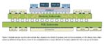
The History of HFSS Meshing

The “Mesh” is the foundation of physics simulation; it’s how a complex modeling problem is discretized into “solvable blocks.” Understandably, for today’s highly complex systems, considerable time may be designated to generating the initial mesh because it’s such a critical step. Accurately capturing the physical geometry under test, as represented by the initial mesh, has a defining influence on the resulting simulation and speed of results. That wasn’t always the case. 25 years ago, simulation was dominated by the actual solving of the electromagnetic fields, and meshing amounted to a tiny fraction of the overall time spent generating a simulated model.

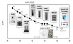
The very first HFSS simulation in 1989 took 16 hours to produce one frequency point on a then-state-of-the-art computer. The vast majority of that 16 hours was spent solving for the electromagnetic fields. Today, we can solve the same model and extract four thousand frequency points in about 30 seconds on an ordinary laptop computer. Advances in speed naturally led engineers to attempt increasingly complex designs through 3D simulation. Over the past 20 years, new meshing technologies supported the pace of innovation, but even with advanced techniques, meshing took up a larger relative portion of the process for complex designs. Simulation technologists saw that meshing was a larger pole in the “simulation tent,” so they introduced new algorithms and parallel processing to encourage further innovation in the simulation space.

Today, Ansys HFSS uses a variety of different meshing algorithms, each optimized for different geometries:

The Original “Classic”

At its core, mesh generation is a space-discretization process where geometry is divided into elemental shapes. While there are several shapes to work with, in HFSS, a mesh represents geometry as a set of 3D tetrahedra, see Figure 1. It can be demonstrated that any 3D shape can be decomposed into a set of tetrahedra. Since HFSS leverages automatic mesh generation, the algorithm makes use of tetrahedra to refine and mathematically guarantee an accurate mesh.

Figure 1: Geometrically conformal tetrahedra leveraged in HFSS automatic mesh generation

Classic is one of Ansys’ earliest meshing technologies. It uses a Bowyer algorithm to create a compact mesh from any set of geometries. It’s an extremely rigorous approach. First, Classic meshes the surfaces of all objects to create a water-tight presentation of the geometry, and then it fills in the volumes of all objects with 3D tetrahedra. For accuracy, mesh elements must be continuous across a surface. In other words, two objects in contact must have a conformal triangular mesh at their adjoining faces. As geometric complexity grew and models started including hundreds or thousands of parts, it became difficult to align the triangular mesh to achieve conformal mesh everywhere. At some point, this meshing approach, which is not readily parallelized, reaches its limit. It can’t handle high levels of design complexity in a reasonable amount of time.

TAU

In 2009, Ansys released the TAU meshing algorithm. TAU approaches the task of meshing from an inverse perspective. From a bird’s-eye view, a model represents some volume of objects potentially contacting others at different points. TAU breaks up the volume into gradually smaller tetrahedra to fit each object in the model. Then, it adaptively refines and tightens local mesh size and shape to align the volumetric mesh with the faces of the input model. Eventually, TAU gets the tetrahedra close enough to each surface for a water-tight mesh that accurately represents all the geometry. For 3D CAD, such as a model of a backplane connector or an aircraft body, TAU is a very robust and reliable algorithm; however, TAU struggles with designs that include high aspect ratio geometries, like PCBs and wirebond packaging, where Classic may perform better.

Both Classic and TAU meshers are designed to handle all arbitrary geometries accurately. Depending on the model, in “Auto-mesh” mode, HFSS determines the correct mesher choice to apply.

Phi Mesher

2013 brought the next generation of meshing at Ansys—Phi. Phi is a layout-based meshing technology that’s 10, 15, or even 20 times faster than previous meshing technology, depending on the model’s geometry. A faster initial mesh often ensures faster simulations; they can be accelerated and enhanced even further with HPC.

Phi is HFSS’ first “geometry-aware” meshing technology. It relies on the layered nature of design that’s commonly found in PCBs or IC packages. The technique is based on the knowledge that all geometry in these kinds of models have a 2D layer description, with the third dimension achieved by sweeping the 2D layer description (in the XY plane) uniformly in Z. Phi was designed to accelerate initial mesh generation by conquering a 3D problem with a 2D approach. It was initially implemented in the HFSS 3D Layout design flow and eventually extended to the 3D workflow a few releases later.

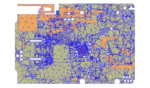
Phi performance is exceptional, achieving speeds an order of magnitude greater than other meshing technologies. In complex IC designs, see Figure 2, it’s a game changer. With earlier techniques, on-chip passive components, for example, took a considerable amount of time to complete. With Phi meshing, an hours-long initial mesh processes can be reduced to minutes or even seconds. However, Phi’s uniform-in-Z constraint limits the types of designs it can handle. For example, Phi can’t be leveraged if trace etching or bondwires were included in IC package design.

 Figure 2: A typical complex PCB design, Phi mesh

That said, with the right geometry, Phi is extremely fast. Once the initial mesh is completed, the adaptive meshing algorithm works the same way as it would with any other HFSS meshing technology to produce the final convergence. In addition, Phi can create a smaller initial meshing count, which contributes to better downstream performance in the adaptive meshing and frequency sweeps. It’s faster from start to finish, not just in the initial mesh generation phase.

The Three Mesh Paradigm

With three meshing technologies in place, an Ansys auto-mesh algorithm scanned model geometries to determine which of the mesh technologies to use. In addition, fallbacks from one meshing technology to another ensured a reliable meshing flow. For example, if the algorithm identified a significant amount of high-aspect-ratio CAD, it would launch the Classic mesh algorithm. Phi was fully automated in the sense that it was always applied to uniformly swept in Z geometry.

Early on, each customer’s design flow tended to align with the same meshing techniques for every project, so they consistently gravitated to one meshing approach. However, as the HFSS solver algorithms became faster and more scalable, and cluster and Cloud hardware became more readily available, the size of HFSS simulations grew and became more complex. Designs were no longer single components; they were systems made up of multiple types of CAD. It wasn’t enough to solve just the PCB or just the connector anymore. To get it right, especially as data rates increased, it became more and more important to simulate together—connector and PCB, antenna and airframe, and so on.

As engineers design for tighter margins in the competitive electronics landscape, simulations encompass the PCB, IC packaging, connectors, surface mount components, and beyond. The Three Mesh Paradigm carried heavy burdens for customers and Ansys alike; a one-mesh-fits-all approach was not optimally effective. Understanding the different options and mesh technologies and knowing when to apply them could be a real challenge.

Enter HFSS Mesh Fusion.

The Rise of HFSS Mesh Fusion

Introduced in early 2021, HFSS Mesh Fusion achieved a fundamental meshing breakthrough using locally defined parameters. In other words, HFSS Mesh Fusion applies meshing technology depending on the local needs of the CAD. For example, when analyzing a simulation where a PCB contains both wirebond packaging and 3D connector models, such as a backplane connector, the PCB portion calls for Phi, wirebond packages call for Classic, and connectors are best meshed using TAU.

This multi-mesh capability became possible with HFSS Mesh Fusion. The only requirement is to assemble the design as a set of 3D Components, which can be encrypted to hide intellectual property and enable easy collaboration with component vendors. The 3D Component hierarchy provides the localized CAD definition to appropriately apply mesh. In addition, the same auto-mesh technology can be used to set the mesh locally, requiring little to no user input. From there, the same adaptive meshing scheme is applied to provide HFSS gold-standard accuracy and reliability.

Ansys recently worked with a team integrating a 5G chipset into a tablet computer. Before Mesh Fusion, there were a lot of mesh challenges to resolve before arriving at a usable simulation. With Mesh Fusion, Phi was applied locally to the chipset and TAU was applied to the remainder of the design—a sleek housing with complex CAD to encase the rest of the electronics in the tablet. Local mesh application ensured a clean mesh on the chipset, which was critical to the accuracy of the overall simulation. All of these seemingly disparate meshing approaches came together in Mesh Fusion for a fast, accurate, and reliable simulation result.

The Future of Meshing at Ansys

The presence of HFSS Mesh Fusion offers a night and day difference for Ansys customers. Instead of getting bogged down by meshing issues to resolve, users are free to explore more intensive design challenges that drive the electronics industry forward.

Most recently, Ansys used a ground-up approach to develop a new meshing technology. This new mesher, called Phi Plus, was designed specifically for wirebond packaging, see Figure 3., which is particularly difficult to mesh with other technologies – even Mesh Fusion. Like Phi, it’s geometry aware and takes advantage of a priori knowledge of system design. In addition, it was developed with parallelization approaches in mind, allowing for excellent scaling with HPC resources. Its success is not limited to wirebond packaging. Phi Plus can handle any kind of combined layout and 3D CAD simulation, such as connector on PCB. Phi Plus meshing is the next game changer in a long line of innovative techniques from Ansys!

Figure 3: Phi Plus Mesh applied to a wire bind package design

For updates, keep an eye on our social channels in this new year.

Also Read

The 5G Rollout Safety Controversy

Can you Simulate me now? Ansys and Keysight Prototype in 5G

Cut Out the Cutouts