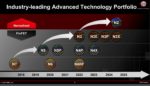
The burgeoning use of conversational artificial intelligence (CAI) in consumer and business applications places a heavy computational burden on both front-end and back-end systems that provide the natural language processing (NLP). NLP systems rely on deep learning (a subset of machine learning) to automate speech recognition, perform the NLP functions, and then provide the text to speech output. To cut costs of the NLP systems, Achronix and Myrtle.ai have partnered, promising to cut costs by 90% as well as reducing the hardware requirements, described in this whitepaper.
Myrtle.ai, a technology specialist in FPGA AI inferencing, implements performant recurrent neural networks (RNN)-based networks on FPGAs using their MAU inferencing acceleration engine. The MAU engine, integrated into the Achronix Speedster®7t AC7t1500 FPGA, leverages key architectural aspects of the Speedster7t architecture to drastically increase the acceleration of real-time automatic speech recognition (ASR) neural networks. That translates into a 2500% increase in the number of real-time streams that can be processed when compared to a server-class CPU.
The CAI pipeline is often defined by three key functional blocks:
- Speech to text (STT), also known as automatic speech recognition (ASR)
- Natural language processing (NLP)
- Text to speech (TTS) or speech synthesis
Such pipelines are found in the millions virtual voice assistants such as Apple’s Siri or Amazon’s Alexa, or voice search assistants on laptops such as Microsoft’s Cortana, as well as automated call center (or contact center) agents and many other applications. The deep learning algorithms that power these CAI services are either processed on the local electronic device or aggregated in the cloud for remote processing at scale. Large-scale deployments supporting millions of consumer interactions represent extremely large compute processing challenges that hyperscaler providers have addressed by developing specialized silicon devices to address the processing of these services.
State of the art ASR algorithms are implemented with end-to-end deep learning. Recurrent neural networks (RNN), unlike convolutional neural networks (CNNs), are common in speech recognition. As noted in “CNN vs. RNN: How are they different?” by David Petersson from TechTarget. RNNs are better suited for processing temporal data, aligning well with ASR applications. RNN-based models require high compute capabilities and high memory bandwidths to process the neural network model within the strict latency targets required for conversational systems. When real-time or automated responses are too slow, the system appears sluggish and unnatural. Often low latency is only achieved at the expense of the processing efficiency which pushes up costs and can become too large for practical deployment.
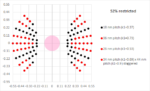
Competing FPGA architectures in the ML acceleration segment claim teraoperations/second (TOPS) rates for inferencing as high as 150 TOPS. Yet in real-world applications, especially those which are latency sensitive such as ASR, these FPGAs fall well short of their headline TOPS rates due to their inability to efficiently transfer data between the compute and external memory. The Achronix Speedster7t architecture strikes the right balance of compute engines, eight high-speed memory interfaces (4 Tbit/s GDDR6 memory interfaces) and high-throughput data transfers (20 Tbit/s network on chip), yielding a device that can deliver 64% of the headline TOPS rates for real- time, low-latency ASR workloads (see the figure).
At the heart of the Speedster 7t architecture are the 2560 machine-learning processor (MLP) blocks. These blocks contain an optimized matrix/vector multiplication function capable of 32 multiplies and one accumulate in a single clock cycle. This is the foundation for the compute engine architecture. Block RAM (BRAM) is co-located with each of the 2560 instances of the MLPs in the AC7t1500, which equates to lower latency and higher throughput. Myrtle.ai’s MAU low latency, high throughput ML inferencing engine has been integrated into the Achronix Speedster7t FPGA, leveraging 2000 of the 2560 MLPs. Because the MLP is a hard block, it can run at a much higher clock rate than if implemented in the FPGA fabric itself.
Most ASR solutions offered by large-scale cloud service providers such as Google, Amazon, Microsoft Azure, and Oracle allow service providers to build products on top of these cloud APIs. However, the service providers face increasingly large bills as their operations scale out, and those products achieve success in the market.
The publicly advertised cost of the larger ASR providers range from $0.01 to $0.025 per minute, and Industry reports suggest that the average call center call is approximately five minutes. Consider a large enterprise data or call center services company fielding 50,000 calls per day at five minutes per call. At the stated rates above, the cost of the ASR processing would range from $1,500 to $6,000 per day or $500,000 to $2,000,000 per year. The Achronix and Myrtle.ai solution can support 4000 RTS on one accelerator card, delivering the capacity to handle over one million calls per day.
There are many factors that would dictate the cost of a stand-alone ASR appliance. For this particular example, assume the Achronix ASR acceleration solution delivered on an FPGA-based PCIe card integrated into an x86-based 2U server. Sold from a system integrator, this appliance might be $50,000 and the annual cost of running the server could double that cost. This leads to $100,000 for the first year for an on-premise ASR appliance. Comparing this on-premise solution versus cloud API services, the end user can enjoy a savings of 5X to 20X in the first year.
Achronix and Myrtle.ai are teaming up to deliver an ASR platform consisting of a 200W, x16 PCIe Gen4-based accelerator card and the associated software which together can sustain up to 4000 RTS concurrently, processing up to 1 million five-minute transcriptions per 24-hour period. Comparing this PCIe accelerator card on a single ×86 server to the cost of cloud ASR services, the first year CAPEX and OPEX can be reduced by as much as 90%.
To download the full whitepaper, visit achronix.com.
Also read:
Benefits of a 2D Network On Chip for FPGAs