Recently, Daniel Nenni blogged on the presentation Wally Rhines gave at #56th DAC. Daniel provided a great summary, but I want to dive into a portion of the presentation in more detail. I love Wally’s presentations, but sometimes you cannot absorb the wealth of information he provides when you initially see it. It’s like getting a huge download from the Hubble Telescope – it takes time to understand what you have just seen or heard.

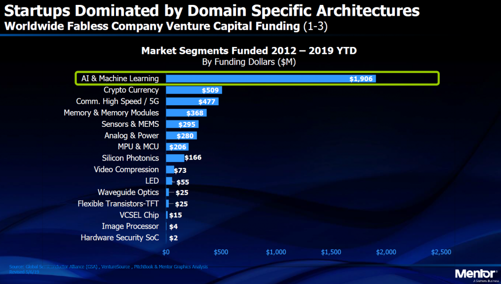
One of the primary points of the presentation was looking at all the money and effort going into AI and machine learning (ML). From 2012 to 2019 this segment has received nearly 4x the amount of investment capital as the next largest category – nearly $2B. Part of the reason for this huge investment is the vast number of solutions that can be developed using AI/ML techniques to run int the cloud – there are many companies developing solutions to different problems. Solving different problems requires different solutions that are coming in the form of application specific processors.
Why application specific processors? For the same reason you would use both a CPU and a GPU – they are optimized to solve different problems and these problems need a lot of computing power to solve their specific tasks making efficiency paramount. Wally even listed some of the myriad solutions for these processors: Vision/Facial Recognition, Voice/Speech/Sound Pattern Recognition, ADAS, Disease diagnosis, Smell/Odor recognition, Robotics/Motion Control/Collision Avoidance, and many more.
So, what is the role of EDA in getting these new chips to market? First, most are being designed at start-ups and systems companies, not semiconductor companies. While it could mean they don’t have much history of chip design, it also means they are more likely to adopt new design techniques more rapidly. My expectation is this will to an accelerating use of high-level synthesis (HLS), prototyping, and emulation. This is because they are developing new types of processors, driving a need to experiment and iterate the design architecture very rapidly while also enabling hardware/software co-design as early as possible.
More information has been coming out on AI/ML solutions in the cloud. Google has announced its Google Cloud AI product which promises to deliver its Tensor Processing Units (TPUs) in the cloud for everyone. Microsoft has deployed Azure Machine Learning and Azure Databricks as another cloud-based AI/ML solution. And there are many others including IBM, Amazon, Oracle, and even Salesforce for use with its applications. These are system companies that are increasingly building more of their own chips.
While much of this entry is focusing on the cloud, the other end of the IoT food chain is also evolving. Confusing to some, the edge devices are starting to look much more complex than expected. These devices will look like small boards, probably with system-in-package chips (SIPs), simply because it is not practical to try to put the compute, memory, radio, and sensor technologies on a single die. More computing at the edge can mean fewer data to transmit and store in the cloud. The tradeoff here is power since many edge devices are battery powered. Some are not those such as in industrial automation or in robotics where the brain is not the portion drawing most of the power. I would expect to see new standards evolve in this area soon in order to facilitate design and interoperability.
Wally, thanks for the insights and information! You keep us aware in interesting times.
Share this post via:


Comments
There are no comments yet.
You must register or log in to view/post comments.