You are currently viewing SemiWiki as a guest which gives you limited access to the site. To view blog comments and experience other SemiWiki features you must be a registered member. Registration is fast, simple, and absolutely free so please,
join our community today!
In a power hungry world of semiconductor devices, multiple ways are being devised to budget power from system to transistor level. The success of IoT (Internet of Things) Edge devices specifically depend on lowest power, lowest area, optimal performance, and lowest cost. These devices need to be highly energy efficient for sustained… Read More
The TSMC quarterly conference call was last week and of course it stirred up quite a bit of controversy. Let me share with you my experience, observations, and opinions and maybe together we can come up with an accurate prediction for 2016. First let’s take a look at 20nm and what people now call the “Apple effect.”
Correct… Read More
IBM recently disclosed a working 7nm test chip generating a lot of excitement in the semiconductor industry and also in the mainstream media. In this article I wanted to explore the 14nm, 10nm and 7nm nodes, the status of the key competitors at each node and what it may mean for the companies.
…
Read More
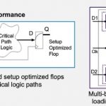
My first exposure to automating IC layout was back in the 1980’s at Intel where I coded a layout compiler to auto-generate about 6% of a graphics processor chip. The need to use automation for IC layout continues today, and with the advent of FinFET technology there are some new challenges like layout gradient effects that … Read More
I talked recently about the Intel acquisition of Altera which seems to be all about using FPGA technology to build custom accelerators for the datacenter. Some algorithms, especially in search, vision, video and so on map much better onto a hardware fabric than being implemented in code on a regular microprocessor.
So if the heart… Read More
In an overwhelmingly digital world, there is a constant cry about the analog design process being slow, not automated, going at its own pace in the same old fashion, and so on. And, the analog world is not happy with the way it’s getting dragged into imperfect automation so it can be more like the digital world. True, the analog world… Read More
Electronics is unusually an evergreen industry where companies make profit, yet end-product prices go down significantly after a brief period of price skimming. A product phases out quite fast (in case of smartphones every 1.5 to 2 years), but still yields big bucks for successful companies in its value-chain. How does this happen?… Read More
Intel’s 10nm may be reliving the 14nm elongated delay issue-
Schedules & tool delivery may be pushed even deeper into 2016-
Meanwhile Samsung & TSMC press on-
Could Intel be embarrassed?
… Read More
If you really want to know why I write about TSMC it is all about ego, my massive ego, absolutely. Blogs about TSMC and the foundries have always driven the most traffic and they most likely always will. Semiconductor IP is second, Semiconductor Design is third, and I don’t think that is going to change anytime soon:
SemiWiki BI: Daniel… Read More
DAC is a great place to gather information about products and technologies. However it can be difficult to chase down the information you need because you may need to cover a lot of ground to hear or talk to the people with the right knowledge. Fortunately there are a few places you can go to learn about a number of products at one place.… Read More