You are currently viewing SemiWiki as a guest which gives you limited access to the site. To view blog comments and experience other SemiWiki features you must be a registered member. Registration is fast, simple, and absolutely free so please,
join our community today!
Successful projects leverage the investment in comprehensive methodology and resource planning, covering design and analysis flows – that planning effort is especially important for functional verification.
The emergence of complex SoC designs for advanced automotive applications has led to a major focus on verification… Read More
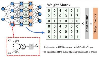
Machine learning applications in data centers (or “the cloud”) have pervasively changed our environment. Advances in speech recognition and natural language understanding have enabled personal assistants to augment our daily lifestyle. Image classification and object recognition techniques enrich our social media experience,… Read More
The user group events held by EDA companies offer a unique opportunity to hear from designers and CAD engineers who are actually using the EDA tools “in the trenches”. Some user presentations are pretty straightforward – e.g., providing a quality-of-results (QoR) design comparison when invoking a new tool feature added to a recent… Read More
Over the past 50 years in our industry, there have been three invariant principles:
- Moore’s Law drives the pace of Si technology scaling
- system memory utilizes MOS devices (for SRAM and DRAM)
- computation relies upon the “von Neumann” architecture
…
Read More
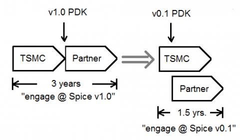
Each year, TSMC hosts two major events for customers – the Technology Symposium in the spring, and the Open Innovation Platform Ecosystem Forum in the fall. The Technology Symposium provides updates from TSMC on:
… Read More
The traditional metrics for evaluating IP are performance, power, and area, commonly abbreviated as PPA. Viewed independently, PPA measures can be difficult to assess. As an example, design constraints that are purely based on performance, without concern for the associated power dissipation and circuit area, are increasingly… Read More
Designers require comprehensive logical, physical, and electrical models to interpret the results of full-chip power noise and electromigration analysis flows, and subsequently deduce the appropriate design updates to address any analysis issues. These models include: LEF, DEF, Liberty library models (including detailed… Read More
One of my favorite traditions at the Design Automation Conference is the Synopsys foundry events (the videos are now available). I learned a long time ago that the foundries are the foundation of the fabless semiconductor ecosystem and your relationships with the foundries can make or break you, absolutely. I also appreciate … Read More
An update on the Design Productivity Gapby Tom Dillinger on 08-03-2018 at 12:00 pmCategories: Cadence, EDA
Over a decade ago, a group of semiconductor industry experts published a landmark paper as part of the periodic updates to the International Technology Roadmap for Semiconductors, or ITRS for short (link). The ITRS identified a critical design productivity gap. The circuit capacity afforded by the Moore’s Law pace of technology… Read More
With the increasing complexity and diversity of the mechanical constraints and electrical requirements in electronic product development, printed circuit board designers are faced with a number of difficult challenges:
- generating accurate (S-parameter) simulation models for critical interface elements of the design
…
Read More


