State-of-the-art chips will always include some portions which are memory arrays, which also happen to be the densest portions of the chip. Arrayed features are the main targets for lithography evaluation, as the feature pitch is well-defined, and is directly linked to the cost scaling (more features per wafer) from generation… Read More
Tag: semiconductors
Wally Rhines: Mentoring Generations of Semiconductor and EDA Professionals
I had the good fortune to catch a live webinar recently that was quite compelling – Conversation with Dr. Walden Rhines: Predicting Semiconductor Business Trends After Moore’s Law! Dr. Rhines, known to most as Wally, doesn’t need much of an introduction. Any semiconductor or EDA professional knows who he is and what he’s accomplished.… Read More
Webinar: Design Methodologies for Next-Generation Heterogeneously Integrated 2.5/3D-IC Designs
I had the opportunity to preview the upcoming SemiWiki webinar titled: Design Methodologies for Next-Generation Heterogeneously Integrated 2.5/3D-IC Designs. John Park’s message, describing this powerful Cadence solution, really impressed me. That’s why I want to encourage you to register for it and join this SemiWiki … Read More
Why I’m Lowering Semiconductor Equipment Revenue Growth to -6.9% in 2020
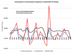
Because of significant $4 billion in equipment pull-ins in Q4 from sales in Asia, I was reducing my semiconductor wafer front-end (WFE) equipment revenue growth from an earlier +5% to 0% in 2020. Now, based on CORVID-19, I am further reducing revenue growth to -6.9%.
Chart 1 also shows the cyclical nature of semiconductors and semiconductor… Read More
Newsflash Chip Equip Blockade Back on!
Blocking chip sales to Huawei back on front burner
Covid19 & China Trade are equally bad
Long lived Uncertainty could “plague” industry sales going forward
Political Predictability worse than Disease Predictability
Reuters broke a story today that the proposed licensing of chip equipment to prevent “bad… Read More
COVID-19 Chip Cycle – How deep, long and what shape?
It is a demand driven downturn – harder to predict
It may not be “business as usual” after this virus
What systemic changes could the industry face?
Trying to figure out another cycle-driven by inorganic catalyst
Investors and industry participants in the semiconductor industry who are used to normal cyclical… Read More
Low Energy Electrons Set the Limits for EUV Lithography
EUV lithography is widely perceived to be the obvious choice to replace DUV lithography due to the shorter wavelength(s) used. However, there’s a devil in the details, or a catch if you will.
Electrons have the last word
The resist exposure is completed by the release of electrons following the absorption of the EUV photon.… Read More
A Conversation with Wally Rhines: Predicting Semiconductor Business Trends After Moore’s Law
Wally Rhines is one of the most prolific speakers the semiconductor industry has ever experienced. Wally is also one of the most read bloggers on SemiWiki.com, sharing his life’s story which is captured in his first book: From Wild West to Modern Life the Semiconductor Evolution.
On April 2nd at 10am PDT we will host Wally on a live… Read More
Semiconductor COVID-19 Update!
Last week whilst China started to recover from COVID-19 outbreak, the rest of the world was seriously impacted by the growing number of cases as the number of cases and deaths outside of China grew higher than in China. With the rise, many governments around the world belatedly put in measures to prevent the further spread of the … Read More
TSMC 32Mb Embedded STT-MRAM at ISSCC2020
32Mb Embedded STT-MRAM in ULL 22nm CMOS Achieves 10ns Read Speed, 1M Cycle Write Endurance, 10 Years Retention at 150C and High Immunity to Magnetic Field Interference presented at ISSCC2020
1. Motivation for STT-MRAM in Ultra-Low-Leakage 22nm Process
TSMC’s embedded Spin-Torque Transfer Magnetic Random Access Memory (STT-MRAM)… Read More


