You are currently viewing SemiWiki as a guest which gives you limited access to the site. To view blog comments and experience other SemiWiki features you must be a registered member. Registration is fast, simple, and absolutely free so please,
join our community today!
Round #1 was here.
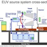
In the EUV corner were Stefan Wurm of Sematech (working on mask issues mostly) and Skip Miller of ASML who are the only company making EUV steppers (and light sources, they acquired Cymer).
You may know that the biggest issue in EUV is getting the source brightness to have high enough energy that an EUV stepper has … Read More
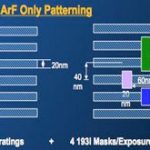
If you want to know the state of play in lithography, there is no better place than the special session on lithography at Semicon West. This year was no exception. The session was given the punchy title Still a tale of 2 paths: multi-patterning lithography at 20nm and below: EUVL source and infrastructure progress.
In the blue corner… Read More
The opening keynote to this year’s Semicon West was by Ajit Manocha, the CEO of GlobalFoundries entitled Foundry-driven Innovation In the Mobility Era. It is no secret that mobile applications, especially smartphones and tablets, are the most significant semiconductor market today. It is not just large, it is disruptive.… Read More
A Goldmine of Tester Databy Beth Martin on 07-10-2013 at 2:06 pmCategories: EDA
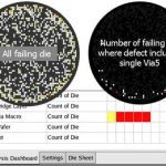
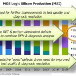
Yesterday at SEMICON West I attended an interesting talk about how to use the masses of die test data to improve silicon yield. The speaker was Dr. Martin Keim, from Mentor Graphics.
First of all, he pointed out that with advanced process nodes (45nm, 32nm, and 28nm), and new technologies like FinFETs, we get design-sensitive defects.… Read More
At Semicon yesterday I attended Mentor’s presentation on improving test standards. Joe Sawicki was meant to present but he was unable to get a flight due to the ongoing disruption at SFO after last weekend’s crash. I just flew in myself and it is odd to see the carcase of that 777 just beside the runway we landed on.
The … Read More
SEMICON West is next week, July 9-11 in San Francisco. If you haven’t signed up, and want to attend for free instead of $100,
1) Send an email to silicon_test@mentor.com with subject line “Semicon pass.”
2) Register for SEMICON West
3) After registering, download the SEMICON West mobile app and start building your schedule. Here… Read More
I will be at Semicon West from 9th to 11th July in Moscone, San Francisco. Of course there are lots of interesting sessions but here are two that I think are especially important to get a good impression of the way things are going in the future from experts. The two most interesting questions about the future are what comes after 14nm,… Read More
EUV is the great hope for avoiding having to go to triple (and more) patterning if we have to stick with 193nm light. There were several presentations at Semicon about the status of EUV. Here I’ll discuss the issues with EUV lithography and in a separate post discuss the issues about making masks for EUV.
It is probably worth … Read More
One of the presenters at the standing-room only litho session at Semicon this week was Serge Tedesco, the litho program manager at CEA-Leti in Grenoble France. He is running a program called IMAGINE for maskless lithography. Chips today are built using a reticle (containing the pattern for that layer of the chip) which is exposed… Read More


