You are currently viewing SemiWiki as a guest which gives you limited access to the site. To view blog comments and experience other SemiWiki features you must be a registered member. Registration is fast, simple, and absolutely free so please,
join our community today!
IBM and Leti each presented several papers at IEDM including a joint nanosheet paper. I had the opportunity to sit down with Huiming Bu, director of advanced logic & memory tech and Veeraraghavan Basker, senior engineer from IBM and then in a separate interview Francois Andrieu, head of advanced CMOS laboratory and Shay Reboh,… Read More
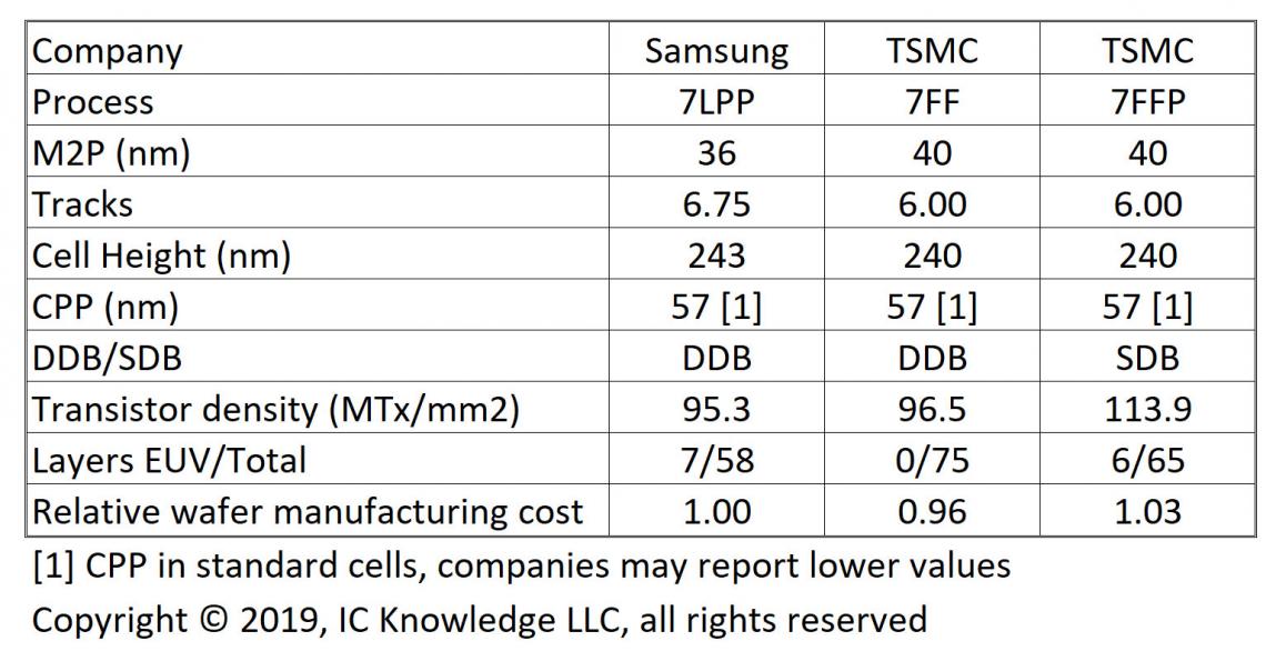
Samsung and TSMC have both made recent disclosures about their 5nm process and I though it would be a good time to look at what we know about them and compare the two processes.
A lot of what has been announced about 5nm is in comparison to 7nm so we will first review 7nm.
7nm
Figure 1 compares Samsung’s 7LPP process to TSMC’s 7FF and 7FFP… Read More
Next week is SPIE, the leading lithography networking event here in Silicon Valley. Scott Jones is not only attending but also presenting at the 15th Annual LithoVision on Sunday. I will be at SPIE as well so if you want to meet up let us know. We will publish a blog on Scott’s presentation the morning of for those who cannot attend.… Read More
I was invited to give a talk at this year’s ISS conference, the talk seemed to be very well received and I was asked to blog about it for SemiWiki. Parts of the talk will be familiar to SemiWiki readers from some of my previous blogs but I also went into more detail around some scaling challenges. The following is a summary of what… Read More
Back in my IP days we spent a lot of time with the ASIC companies chasing multi-million dollar licensing deals. IBM was a fierce ASIC competitor back then with leading edge processes and a silicon proven IP catalog that was unmatched.
Unfortunately that ended at 65nm as the pure-play foundries (TSMC and UMC) and fabless ASIC companies… Read More
For more than a decade 2D NAND has been the leading driver of lithography shrinks, for example, Samsung went from 120nm in 2003 to 16nm in 2014 with shrinks on an almost yearly basis, but the shrinks came at a price. At 16nm Self Aligned Quadruple Pattering (SAQP) was required for the most critical layers and patterning related costs… Read More
An interesting thing happened during the driving tour of the GlobalFoundries Fab 8 in Malta, NY. We happened by an old structure with quite a bit of history. As it turns out, the “Malta Test Station”, a former US Army fuel and explosives testing facility, was the actual birthplace of the United States’ Space & Missile programs.… Read More