You are currently viewing SemiWiki as a guest which gives you limited access to the site. To view blog comments and experience other SemiWiki features you must be a registered member. Registration is fast, simple, and absolutely free so please,
join our community today!
Lurking inside of every Mosfet is a parasitic bipolar junction transistor (BJT). Of course, in normal circuit operation the BJT does not play a role in the device operation. Accordingly, SPICE models for Mosfets do not behave well when the BJT is triggered. However, these models work just fine for most purposes. The one important… Read More
New products always take precedence since EDA is a “mature” market. I have inside knowledge on this one so I can tell you it is not to be missed. Coincidently, but not really, a related white paper was just published so if you are not going to 56thDAC you can still get a virtual briefing. If you are going to DAC be sure and stop by the Fractal… Read More
The letters “PVT” roll of the tongue easily enough, belying the complexity that variations in process, temperature and voltage can cause for analog designs. For semiconductor processes, there are dozens of parameters that can affect the viability of a design. It would be easy enough to optimize a circuit with only one or two varying… Read More
At the beginning of every project the one of the first questions that ought to be asked is whether there blocks from previous designs that can be reused. On the surface this seems pretty obvious. The wrinkle in this is that reusability varies a lot based on the design type and the effort that a team is willing to expend to bring a design… Read More
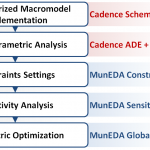
When working on an analog design, after initial design specs have been met, it is useful to determine if the design meets specs out to 3 or 4 sigma based on process variation. This can serve as a useful step before going any further. It might not be a coincidence that foundries base their Cpk on 3-sigma. To refresh, Cpk is the ratio of the… Read More
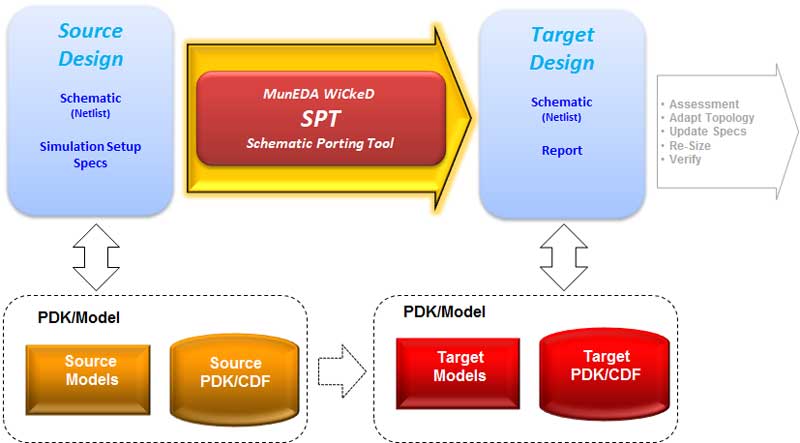
Schematics are still the lynchpin of analog design. In the time that HDL’s have revolutionized digital design, schematics have remained drawn and used much as they have been for decades. While the abstraction of HDL based designs has made process and foundry porting relatively straightforward, porting schematic based designs… Read More
Configurable analog IP has traditionally been a tough nut to crack. Digital IP, of course, now provides for wide configurability for varying applications. In the same way that analog design has remained less deterministic as compared to digital design, analog IP has also tended to be less flexible. However, the tide may be turning… Read More
Optimizing analog designs has always been a difficult and tricky process. Designing for IoT applications has only made this more difficult with the added importance of minimizing power. Unlike other circuit parameters, it is not easy to specify power as a design goal when using equations. Power is a resultant property and must… Read More
Talking with actual IC designers is always fascinating to me, because these engineers are the unsung heroes that enable our modern day world of consumer and industrial electronics. Too often we only hear from the CEO or other C-level executives in the press about their own companies, products, services and vision. I recently had… Read More
Popular companies designing smart phones, CPUs, GPUs and Memory components all employ teams of custom IC designers to create the highest performance chips that are as small as possible, and at the lowest costs. How do they go about doing custom IC design migration and optimization when moving from one process node to another one?… Read More