Webinar: Fast and Accurate High-Sigma Analysis with Worst-Case Points

Webinar: Fast and Accurate High-Sigma Analysis with Worst-Case Points
by Daniel Payne on 11-02-2023 at 10:00 am

Worst case point min

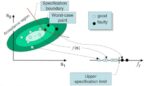
IC designers are tasked with meeting specifications like robustness in SRAM bit cells where the probability of a violation are lower than 1 part-per-billion (1 ppb). Another example of robustness is a Flip-Flop register that must have a probability of specification violation lower than 1 part-per-million (1 ppm). Using Monte… Read More


Analog Circuit Migration and Optimization

Analog Circuit Migration and Optimization
by Daniel Payne on 07-18-2023 at 6:00 am

WiCkeD Flow, analog circuit optimization

The MunEDA User Group Meeting (MUGM)  has been an annual event since 2006, and this year there were some 80 participants from many customers that attended to share their experiences and learn how to get the best EDA tool results. I’ve been able to view the presentations and archived videos, so will share some of the interesting… Read More


Developing the Lowest Power IoT Devices with Russell Mohn

Developing the Lowest Power IoT Devices with Russell Mohn
by Daniel Nenni on 03-24-2023 at 6:00 am

InPlay NanoBeacon Technology

Russell Mohnis the Co-Founder and Director of RF/AMS Design at InPlay Inc. and his team has been using WiCkeD from MunEDA for several years. We thought the rest of the world would like to learn about his experiences.

How did you get started in semiconductors and what brought you to InPlay?
I was initially drawn to analog and mixed-signal… Read More


Webinar: Enhance Productivity with Machine Learning in the Analog Front-End Design Flow

Webinar: Enhance Productivity with Machine Learning in the Analog Front-End Design Flow
by Daniel Payne on 03-23-2023 at 6:00 am

analog Circuit Optimization

Analog IC designers can spend way too much time and effort re-using old, familiar, manual iteration methods for circuit design, just because that’s the way it’s always been done. Circuit optimization is an EDA approach that can automatically size all the transistors in a cell, by running SPICE simulations across… Read More


Webinar: Post-layout Circuit Sizing Optimization

Webinar: Post-layout Circuit Sizing Optimization
by Daniel Payne on 09-29-2022 at 4:00 pm

IC design workflow min

My IC design career started out with manually sizing transistors to improve performance, while minimizing layout area and power consumption. Fortunately we don’t have to do manual transistor sizing anymore, thanks to EDA tools that are quicker and more accurate than manual methods. MunEDA is an EDA vendor that has developed… Read More


Webinar: Simulate Trimming for Circuit Quality of Smart IC Design

Webinar: Simulate Trimming for Circuit Quality of Smart IC Design
by Daniel Nenni on 03-23-2022 at 6:00 am

p1

Advanced semiconductor nanometer technology nodes, together with smart IC design applications enable today very complex and powerful systems for communication, automotive, data transmission, AI, IoT, medical, industry, energy harvesting, and many more.

However, more aggressive time-to-market and higher performance… Read More


WEBINAR: Using Design Porting as a Method to Access Foundry Capacity

WEBINAR: Using Design Porting as a Method to Access Foundry Capacity
by Tom Simon on 11-24-2021 at 8:00 am

Schematic Porting the NanoBeacon

There have always been good reasons to port designs to new foundries or processes. These reasons have included reusing IP in new projects, moving an entire design to a smaller node to improve PPA, or second sourcing manufacturing. While there can be many potential business motivations for any of the above, in today’s environment… Read More


Numerical Sizing and Tuning Shortens Analog Design Cycles

Numerical Sizing and Tuning Shortens Analog Design Cycles
by Tom Simon on 11-22-2021 at 6:00 am

Sizing and tuning

By any measure analog circuit design is a difficult and complex process. This point is driven home in a recent webinar by MunEDA. Michael Pronath, VP Products and Solutions at MunEDA, lays out why, even with the assistance of simulators, analog circuit sizing and tuning can consume weeks of time in what can potentially be a non-convergent… Read More


Webinar on Tools and Solutions for Analog IP Migration

Webinar on Tools and Solutions for Analog IP Migration
by Tom Simon on 03-17-2020 at 10:00 am

MunEDA flow for analog design porting

The commonly advanced reason for IP reuse is lower cost and shorter development time. However, IP reuse presents its own challenges, especially for analog designs. In the case of digital designs, once a new standard cell library is available, it is usually not too hard to resynthesize RTL to create new working silicon. For analog… Read More


56th DAC – In Depth Look at Analog IP Migration from MunEDA

56th DAC – In Depth Look at Analog IP Migration from MunEDA
by Tom Simon on 07-31-2019 at 10:00 am

Every year at DAC, in addition to the hubbub of the exhibit floor and the relatively short technical sessions, there are a number of tutorials that dive in depth into interesting topics. At the 56th DAC in Las Vegas this year, MunEDA offered an interesting tutorial on Analog IP migration and optimization. This is a key issue for large… Read More