You are currently viewing SemiWiki as a guest which gives you limited access to the site. To view blog comments and experience other SemiWiki features you must be a registered member. Registration is fast, simple, and absolutely free so please,
join our community today!
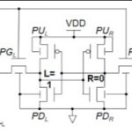
I’ve done SRAM and DRAM design before as a circuit designer from 1978-1986, but in 2016 there are so many more challenges to using 28nm and 14nm on FDSOI technology. One way to keep abreast of SRAM design is to read conference papers, so I just finished a paper from authors at STMicroelectronics and MunEDA presented at the IEEE… Read More
I was born in 1957, the same year that the Soviets launched the first satellite into Earth orbit, officially starting the Space Race between two global super powers. Today there are many countries engaged in space research and I just read about how engineers at IEAv (Institute for Advanced Studies) in Brazil did their IC design optimization… Read More
Analog IP is more difficult to design and optimize for a given process node compared to digital IP, so any automation for analog designers is always welcome. The engineers at SMIC in China have customers that design analog IP and often they need to know how to optimize it for a specific process, so I watched a presentation by Josh Yang,… Read More
As I mentioned in “EDA Dead Pool” acquisitions in our industry will continue at a rapid pace. The latest victim is 10 year old French company Infiniscale who was recently purchased by Silvaco. This was more of a “let’s put your product through our massive sales and support channel” kind of deal so it will be 1 + 1 = 3 accretive for sure.… Read More
Designing Analog IP is often referred to as a “black art”, something that only highly experienced craftsmen can produce using transistor-level techniques that aren’t shared outside of their closely held group of trusted co-workers. I’d like to suggest that Analog IP can be designed and optimized … Read More
My first job out of college was transistor-level circuit design of DRAMs at Intel, so I’ve continued to be fascinated with both the craft and science of designing, optimizing, verifying and debugging custom ICs. Last October I traveled to Munich, Germany to attend a two day user group meeting for engineers using tools from… Read More
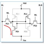
My IC design career started out with DRAM at Intel, and included SRAM embedded in GPUs, so I recall some common questions that face memory IP designers even today, like:
- Does reading a bit flip the stored data?
- Can I write both 0 and 1 into every cell?
- Will read access times be met?
- While lowering the supply voltage does the cell data retain?
…
Read More
There are three critical goals that designers of custom digital designs and memories look to achieve with high sigma verification:
(1) obtaining accurate results,
(2) achieving results with good run-time (efficiency), and
(3) gaining proper insight into how their circuit is behaving along with an understanding of failure … Read More
We have been hearing about low power for a long time. Fortunately, low power chip operation has come about through a large number of innovations. Key among these is clock gating, frequency and voltage scaling, managing leakage with lower threshold voltage, HKMG, and many other techniques. But we are entering the age of ultra low… Read More
Right now I’m typing on my MacBook Pro computer connected to the Internet through WiFi, thanks to the electronics in both my laptop and WiFi router. I kind of take WiFi for granted because it is so ubiquitous throughout my daily life, yet there are IC designers at companies like Lantiq Semiconductorthat have to design and optimize… Read More