You are currently viewing SemiWiki as a guest which gives you limited access to the site. To view blog comments and experience other SemiWiki features you must be a registered member. Registration is fast, simple, and absolutely free so please,
join our community today!
There’s much talk in EDA about High Level Synthesis (HLS), Transaction Level Modeling (TLM) and the Universal Verification Methodology (UVM), however there’s a lower-level of abstraction, the transistor-level, where high-speed digital cell libraries are created, analog circuits are crafted, and AMS designers… Read More
SMIC (Semiconductor Manufacturing International Corporation) is a China-based foundry with technology ranging from 0.35 micron to 28 nm, and we’ve blogged about them before on SemiWiki. I’ve been reading about SMIC recently because they created a technical presentation for the MunEDA Technical Forum Shanghai… Read More
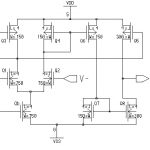
RTL designers know that their code gets transformed into gates and cells by using a logic synthesis tool, however these gates and cells are further comprised of transistors and sometimes you really need to optimize the transistor sizing to reach power, performance and area goals. I’ve done transistor-level IC design before,… Read More
User group meetings are a rich source of information for IC designers because they have actual designers talking about how they used EDA tools in their methodology to achieve a goal. Engineers at STMicroelectronicspresented at a MunEDAUser Group on the topic: I/O Design Optimization Flow For Reliability In Advanced CMOS Nodes.… Read More
So first the one thing that you do know. MunEDA are based in Munich which makes them German. I have to confess that until I got involved helping them a bit with some marketing stuff that that was about all I knew about them too.
So now five things that you might not know:
1. MunEDA have a much wider customer list that you know and would even… Read More
When I hear the phrase “high sigma” I think of the EDA vendor Solido, however at DAC on Monday I visited another EDA company called MunEDAthat has several products of interest to transistor-level IC designers. I was able to speak with three different people from MunEDA and here’s what I learned.… Read More
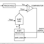
Digital designers have used logic optimization and logic synthesis for decades as a means to produce more optimal designs with EDA tools. On the analog and transistor-level side of design the efforts to automatically optimize for speed or power have generally been limited to circuits with only a handful of transistors. These … Read More
Low Power Designby Paul McLellan on 05-16-2014 at 9:08 pmCategories: EDA, MunEDA
So you want to do a low power design. Join the club. Who doesn’t? Today all designs are low power, it is the biggest constraint on what we can do on a chip. Power down; power domains, variable clock rates, mixed Vt libraries. Every trick is needed. And that is not even enough. We get to put our phones on charge each evening and there… Read More
In 2002, MunEDA was launched under the guidance of EDA academic veterans and IEEE fellows Prof. Kurt Antreich and Prof. Helmut Gräb (TUM Munich Technical University ) which represented 20 plus years of EDA research and experience. All MunEDA tools are combined in a tool suite called WiCkeD[SUP]TM[/SUP]. The tool suite brand was… Read More
Last week Berkeley Design Automation introduced a new Analog Characterization Environment (ACE) – a high-productivity system to ensure analog circuits meet all specifications under all expected operational, environmental, and process conditions prior to tapeout.
While standard cell characterization and memory characterization… Read More