You are currently viewing SemiWiki as a guest which gives you limited access to the site. To view blog comments and experience other SemiWiki features you must be a registered member. Registration is fast, simple, and absolutely free so please,
join our community today!
The IEEE International Electron Devices Meeting is in my opinion the leading technology conference to understand the current state-of-the-art in semiconductor process technology. Held each year in early December in San Francisco it is a must attend conference for anyone following technology development. The following is… Read More
(Adapted from a presentation first given under this title in 1989 and subsequently expanded in presentations over a period of nearly thirty years)
In 1965, Gordon Moore, then R&D Manager for Fairchild Semiconductor, published a paper in “Electronics” magazine predicting the trend for semiconductors in the next ten years. … Read More
The pace of Moore’s Law scaling for monolithic integrated circuit density has abated, due to a combination of fundamental technical challenges and financial considerations. Yet, from an architectural perspective, the diversity in end product requirements continues to grow. New heterogeneous processing units are being… Read More
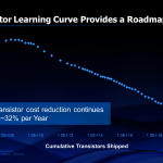
Figure 1 is the most basic of all the predictable parameters of the semiconductor industry, even more so than Moore’s Law. It is the learning curve for the transistor. Since 1954, the revenue per transistor (and presumably the cost per transistor, if we had the data from the manufacturers) has followed a highly predictable learning… Read More
The Integrated Circuitby John East on 06-10-2019 at 5:00 amCategories: John East
The “20 Questions with John East” series continues
Noyce and the rest of the traitorous eight left Shockley without a clue as to what they would do next. They believed in semiconductors and knew that they were the very best semiconductor guys in the world. Their hope was to find a company who would hire them en masse. After some false… Read More
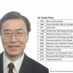
Sometimes we get to see, up close, leaders who make a truly enormous contribution to society. Dr. Sunlin Chou was one such leader and I was a fortunate fellow traveler. Sunlin led the exponential rise of transistors for 35 years, accelerating the waves of revolutionary digital technologies serving humanity.
Fifty years have … Read More
This is what happens when you have a CFO acting as a semiconductor CEO, and Robert Holmes is a career CFO with zero semiconductor experience or education. Granted, no way did he write the opening statement, but it was full of jibber jabber anyway. The real disappointing jibber jabber was from our own Murthy Renduchintala on the status… Read More
ASML reported EUR2.78B in revenues with EUR2.08B in systems. 58% was for memory. EUV was EUR513M with 5 systems. Importantly orders were for EUR2.20B in systems at 64% memory and 5 EUV tools. This was likely better than expectations given the overall industry weakness. EPS of EUR1.60 was more or less in line with expectations. Guidance… Read More
An update on the Design Productivity Gapby Tom Dillinger on 08-03-2018 at 12:00 pmCategories: Cadence, EDA
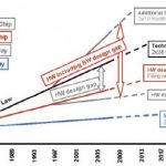
Over a decade ago, a group of semiconductor industry experts published a landmark paper as part of the periodic updates to the International Technology Roadmap for Semiconductors, or ITRS for short (link). The ITRS identified a critical design productivity gap. The circuit capacity afforded by the Moore’s Law pace of technology… Read More
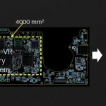
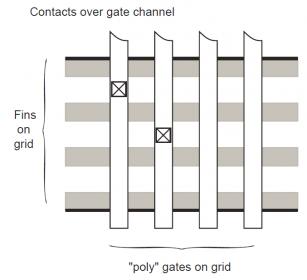
Samsung Foundry recently held their annual technology forum in Santa Clara CA. The forum consisted of: presentations on advanced and mainstream process technology roadmaps; the IP readiness for those technology nodes; a review of several unique package offerings; and, an informal panel discussion with IP designers and EDA… Read More