You are currently viewing SemiWiki as a guest which gives you limited access to the site. To view blog comments and experience other SemiWiki features you must be a registered member. Registration is fast, simple, and absolutely free so please,
join our community today!
In 1991, I arrived in Glasgow to become a lecturer in Glasgow University, attracted by the Silicon Glen – the heart of semiconductor manufacturing in Europe. Here are few facts:
- The larges semiconductor plant in Europe at that time was the NEC DRAM manufacturing site in Livingstone. When I visited the plant, I was mesmerized
…
Read More
A little over a month ago, I wrote about the substantial support that Silicon Catalyst and Arm were providing for chip startups. There have been many incubators for technology companies over the years. These organizations typically provide office space, some basic infrastructure, advisory help and sometimes access to seed … Read More
I enjoy learning and writing about new technologies closely connected to our personal and working lives (the kind you could explain to your Mom or a neighbor). So naturally I’m interested in AI, communication and security as applied to the home automation, transportation, virtual, augmented and mixed reality, industry and so… Read More
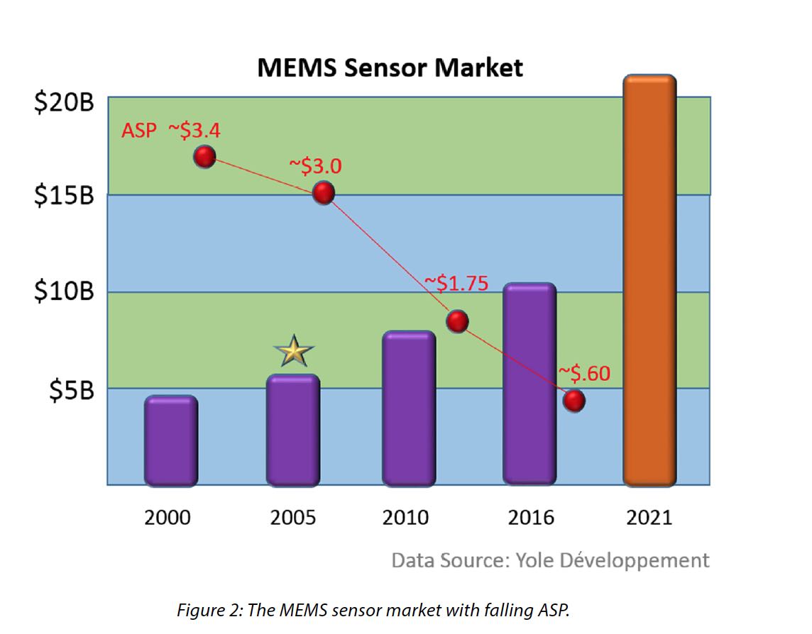
MEMS sensors play a huge role in intelligent systems these days. Mobile and IoT devices would essentially be blind if not for the rich variety of MEMS sensors integrated into them. The MEMS sensor market is growing rapidly, topping $10B in 2016 and slated to exceed $20B by 2020. MEMS is also growing in the RF market, where they are providing… Read More
When it comes to building edge devices for the internet-of-things (IoT), you don’t want to have to break the bank to prototype an idea before diving into the deep water. At the same time, if your idea is to shrink an edge device down to it’s smallest dimensions, lowest power and lowest cost, you really want to be able to prototype your… Read More
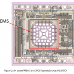
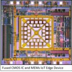
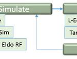
In my 34 years in IC and EDA, it never ceases to amaze me as to how ingenious designers can be with what is given them. Mentor, a Siemens business, has released a wonderful white paper that is proof of this yet again. The white paper steps through how one of their customers, MEMSIC, used the Tanner tool suite to develop a combination CMOS… Read More
There has been quite a bit of coverage on this already but Bosch building a fab in Dresden is a big deal so let me share my experience, observation, and opinion as us bloggers do. The $1.1B question of course is: Why didn’t Bosch invest in GlobalFoundries FD-SOI fabs in Dresden instead? Automotive and IoT is perfect for FD-SOI,… Read More
As I write about integrated photonics I continue to hear from long-time experts in the field who lament that integrated photonics has been around for decades and other than telecom/datacom, it seems to never be a mainstream technology. It’s hard to argue that this time around it will be different as those people have lived through… Read More
Last Friday I learned something new about IoT by attending a SEMI event in Wilsonville, OR just a few short miles away from where I live in Tualatin. SEMI puts on two events here in Oregon each year, and their latest event on IoT Sensors was quite timely and popular judging by how many attendees showed up. First up was Jeff Miller from … Read More
IoT edge device design means four domains – MEMS, analog, digital, and RF – not only work together, but often live on the same die (or substrate in a 2.5D process) and are optimized for power and size. Getting these domains to work together effective calls for an enhanced flow.
Historically, these domains have not played together … Read More