
IoT edge device design means four domains – MEMS, analog, digital, and RF – not only work together, but often live on the same die (or substrate in a 2.5D process) and are optimized for power and size. Getting these domains to work together effective calls for an enhanced flow.
Historically, these domains have not played together in silicon. Designs were executed at a PWB level, bringing together chips with different design rules and packaging technology. This was a risk reduction maneuver; each domain could be debugged more or less independently, then integration issues such as crosstalk, interference, and signal integrity solved using macro techniques for mitigation. Domain experts usually didn’t cross disciplines, except to understand the interfaces between the domains.
Now, interaction between domains is much more critical to success in constrained IoT edge designs. Mixed signal design is pretty much taken for granted now, but more and more people are having success in on-chip RF and MEMS integration. The bar has been raised by better EDA tools that handle a unified flow from capture to simulation to layout.
Note I said tools. It’s not necessarily a single tool, but rather an integrated suite operating from the same data repository with the same user interface that is important. What kills productivity is switching costs. Bringing together these four domains is easier said than done, however. Analog types are used to working in schematics, digital types in RTL, and MEMS and RF designers are often working at the metal layers.
This challenge is really the motivation behind the Mentor Graphics purchase of Tanner EDA a year and a half ago. Integrating those disparate domains and bringing a full suite of EDA tools together in one comprehensive flow is a big job that the Tanner teams have been working on relentlessly since the acquisition. Mentor’s PWB tools such as PADS, created with small teams in mind, also factor in to the flow. For IoT edge devices, it goes even deeper – Mentor’s purchase of CodeSourcery was all about optimizing chips for real-time software.
A new Mentor white paper authored by Jeff Miller has an interesting premise: if we have a better design flow for IoT devices, handling all four domains, we get more optimized parts. (He’s gone as far to suggest there is “a new breed of designers.” That has a lot to do with how engineers come through school. I’m not sure deep expertise in all four domains are possible in a single person, but I am sure that designers are becoming much more familiar with cross-domain design and collaboration in small teams.)
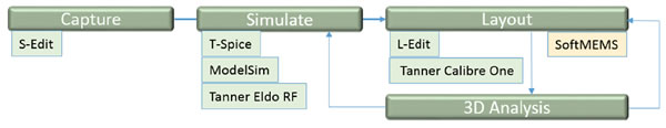
The Tanner IoT design flow handles all the way from capture through simulation to layout:

Miller walks through how the tools tie together in this scenario. His discussion on simulation is particularly interesting. For example, in a mixed-signal simulation, T-Spice and ModelSim work together, passing data back and forth whenever signals change at the analog/digital boundary.
What about the MEMS part of the job? Miller suggests that creating 3D models and then trying to derive a 2D mask is difficult and can lead to errors. He suggests a mask-forward flow, bringing in a 2D mask from Tanner L-Edit and then generating the 3D model. And the RF? Tanner Eldo can be used to analyze RF circuits with several algorithms and help optimize the results for various types of circuits.
Just reading through this discussion, it is clear the different domains call for different handling, and there has been a lot of progress in Tanner EDA tool integration. The entire white paper is available for download (registration required):
Driving Intelligence to the IoT Edge Invents a New Breed of Designers
As I said, I don’t think there is any magic that transforms a single designer into an expert in all four domains just by adding tools. What we are seeing is EDA vendors starting to think about their tools as part of a bigger system design effort with various facets, with a collaborative design team working in one environment with integrated tools.
Share this post via:


Comments
0 Replies to “Can one flow bring four domains together?”
You must register or log in to view/post comments.