You are currently viewing SemiWiki as a guest which gives you limited access to the site. To view blog comments and experience other SemiWiki features you must be a registered member. Registration is fast, simple, and absolutely free so please,
join our community today!
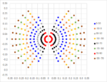
The stochastic nature of imaging has received a great deal of attention in the area of EUV lithography. The density of EUV photons reaching the wafer is low enough [1] that the natural variation in the number of photons arriving at a given location can give rise to a relatively large standard deviation.
In recent studies [2,3], it … Read More
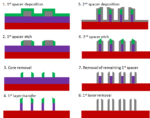
Self-aligned quadruple patterning (SAQP) is the most widely available technology used for patterning feature pitches less than 38 nm, with a projected capability to reach 19 nm pitch. It is actually an integration of multiple process steps, already being used to pattern the fins of FinFETs [1] and 1X DRAM [2]. These steps, shown… Read More
Moore’s Law has been about device density, specifically transistor density, increasing every certain number of years. Although cost is the most easily grasped advantage, there are two other benefits: higher performance (speed) and reduced power. When these benefits are compromised, they can also pose a scaling limitation.
…
Read More
In a previous article [1], the Rayleigh criterion was mentioned as the resolution limit for the distance between two features. On the other hand, in a following article [2], the minimum pitch was mentioned for the resolution limit for arrayed features. In this article, we reconcile the two by considering gaps between arrayed features,… Read More
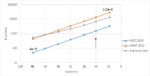
State-of-the-art chips will always include some portions which are memory arrays, which also happen to be the densest portions of the chip. Arrayed features are the main targets for lithography evaluation, as the feature pitch is well-defined, and is directly linked to the cost scaling (more features per wafer) from generation… Read More
As any semiconductor process advances to the next generation or “node”, a sticky point is how to achieve the required higher resolution. As noted in another article [1], multipatterning (the required use of repeated patterning steps for a particular feature) has been practiced already for many years, and many have… Read More
Extreme ultraviolet (EUV) lithography targets sub-20 nm resolution using a wavelength range of ~13.3-13.7 nm (with some light including DUV outside this band as well) and a reflective ring-field optics system. ASML has been refining the EUV tool platform, starting with the NXE:3300B, the very first platform with a numerical
…
Read More
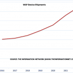
Advanced IC packaging, such as fan-out WLP (Wafer Level Packaging) and 2.5D TSV (Through Silicon Via) will drive the packaging equipment market, particularly lithography. This will help specific equipment manufacturers in 2019, since the WFE (Wafer Front End) market will drop 17%. But the Back-End lithography market, led … Read More
One of the more frequent questions I get, “What is next after FinFETs?” is finally getting answered. Thankfully I am surrounded by experts in the process technology field including Scotten Jones of IC Knowledge. I am also surrounded by design enablement experts so I really am the man in the middle which brings us to a discussion between… Read More
SPIE is the premier event for lithography held in Silicon Valley and again Scotten Jones and I will be attending. EUV is generally the star of the show and this year will be no different now that TSMC has committed to EUV production in 2019.
Last year at SPIE, TSMC presented the history of EUV development from the beginning in 1985 as … Read More