You are currently viewing SemiWiki as a guest which gives you limited access to the site. To view blog comments and experience other SemiWiki features you must be a registered member. Registration is fast, simple, and absolutely free so please,
join our community today!
A few weeks back I wrote an article mentioning that Mentor Graphics has been quietly working on solutions for photonic integrated circuits (PICs) for some time now, while one of their competitors has recently established a photonics beachhead. One of the most common challenges for PIC designs is their curvilinear nature, thus… Read More
Next week is SEMICON West and I plan to be there all week. SEMICON West is a great opportunity to see the latest in equipment and materials on the show floor, to attend all the talks and receptions and to meet with various industry experts.… Read More
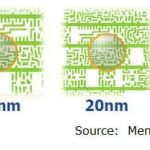
It is truly amazing to consider the advances in microelectronic process development, using 193i photolithography. The figure below is a stark reminder of the difference between the illuminating wavelength and the final imaged geometries. This technology evolution has been enabled by continued investment in mask data generation… Read More
The worldwide revenue of semiconductor industry has remained flat in last few years; to be more precise, overall semiconductor revenue declined by 1.9% in 2015 and Gartner forecasts it to further decline by 0.6% in 2016. The total revenue was at record high of $340.3 billion in 2014.
Well, semiconductor industry has matured. A … Read More
I previously published a summary of day 1 of SPIE and I wanted to follow up with observations from successive days.
SPIE, the international society for optics and photonics, was founded in 1955 to advance light-based technologies.Serving more than 256,000 constituents from approximately 155 countries, the not-for-profit … Read More
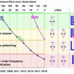
With today’s ArF based lithography using 193nm wavelength light, we are hard up against the limitations imposed by the Raleigh equation. Numerous clever things have been devised to maximize yield and reduce feature size. These include 2 beam lithography, multiple patterning, immersion litho processes to improve NA, thinner… Read More
The 40[SUP]th[/SUP] SPIE Advanced Lithography conference will be at the San Jose Convention Center 22-26 February. Over the past few years, this conference has grown in scope to include emerging patterning technologies, like directed self-assembly (DSA) and design-process-technology co-optimization.
Underlying all … Read More
On the Cadence booth at DAC, Lars Liebmann of IBM presented on the challenges of 10nm. As he put it, how the lithography folks are keeping things very interesting for the EDA tool development engineers. Although 14nm/16nm hasn’t yet ramped into HVM, the advanced work for tools and IP has all moved to 10nm. Although Lars gave… Read More
Shakespeare reckoned that a man went through seven stages in his life.All the world’s a stage, And all the men and women merely players. They have their exits and their entrances, And one man in his time plays many parts, His acts being seven ages.
Well, an EUV mask seems to only go through three main stages:
[LIST=1]
the blank…
Read More
All the details of how we will build semiconductors going forward depend on whether we have EUV in our arsenal or not. Imec is very close to this since they work closely with ASML (who are about an hour and half’s drive away just outside Eindhoven in the Netherlands). At the imec technology symposium we were given a quick summary… Read More