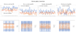
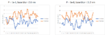
Previously, I had indicated how detrimental stochastic effects at pitches below 50 nm should lead to reconsidering the practical resolution limit for EUV lithography [1]. This is no exaggeration, as stochastic effects have been observed for 24 nm half-pitch several years ago [2,3]. This then leads to the question of whether … Read More

Tag: lithography
Pinning Down an EUV Resist’s Resolution vs. Throughput
The majority of EUV production is on 5nm and 3nm node, implemented by late 2022. Metal oxide resists have not been brought into volume production yet [1,2], meaning that only organic chemically amplified resists (CARs) have been used instead until now. These resists have a typical absorption coefficient of 5/um [3,4], which means
Application-Specific Lithography: Avoiding Stochastic Defects and Image Imbalance in 6-Track Cells
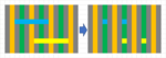
The discussion of any particular lithographic application often refers to imaging a single pitch, e.g., 30 nm pitch for a 5nm-family track metal scenario. However, it is always necessary to confirm the selected patterning techniques on the actual use case. The 7nm, 5nm, or 3nm 6-track cell has four minimum pitch tracks, flanked… Read More
Application-Specific Lithography: Sense Amplifier and Sub-Wordline Driver Metal Patterning in DRAM
On a DRAM chip, the patterning of features outside the cell array can be just as challenging as those within the array itself. While the array contains features which are the most densely packed, at least they are regularly arranged. On the other hand, outside the array, the regularity is lost, but the in the most difficult cases, … Read More
Predicting Stochastic Defectivity from Intel’s EUV Resist Electron Scattering Model
The release and scattering of photoelectrons and secondary electrons in EUV resists has often been glossed over in most studies in EUV lithography, despite being a fundamental factor in the image formation. Fortunately, Intel has provided us with a laboriously simulated electron release and scattering model, using the GEANT4… Read More
ASML- Absolutely Solid Monopoly in Lithography- Ignoring hysteria & stupidity

- This past weeks over-reaction to Canon echoes the Sculpta Scare
- Nanoimprint has made huge strides but is still not at all competitive
- Shows basic lack of understanding of technology by some pundits
- Chip industry has been searching for alternatives that don’t exist
Much ado about nothing much…..
This past week we … Read More
Extension of DUV Multipatterning Toward 3nm
China’s recent achievement of a 7nm-class foundry node using only DUV lithography [1] raises the question of how far DUV lithography can be extended by multipatterning. A recent publication at CSTIC 2023 indicates that Chinese groups are currently looking at extension of DUV-based multipatterning to 5nm, going so far… Read More
Modeling EUV Stochastic Defects with Secondary Electron Blur
Extreme ultraviolet (EUV) lithography is often represented as benefiting from the 13.5 nm wavelength (actually it is a range of wavelengths, mostly ~13.2-13.8 nm), when actually it works through the action of secondary electrons, electrons released by photoelectrons which are themselves released from ionization by absorbed… Read More
Application-Specific Lithography: Via Separation for 5nm and Beyond
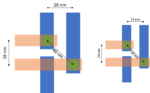
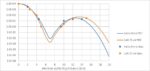
With metal interconnect pitches shrinking in advanced technology nodes, the center-to-center (C2C) separations between vias are also expected to shrink. For a 5/4nm node minimum metal pitch of 28 nm, we should expect vias separated by 40 nm (Figure 1a). Projecting to 3nm, a metal pitch of 24 nm should lead us to expect vias separated… Read More
NILS Enhancement with Higher Transmission Phase-Shift Masks
In the assessment of wafer lithography processes, normalized image log-slope (NILS) gives the % change in width for a given % change in dose [1,2]. A nominal NILS value of 2 indicates 10% change in linewidth for 10% change in dose; the % change in linewidth is inversely proportional to the NILS. In a previous article [2], it was shown… Read More