One of my favorite EDA disruptions is the Siemens acquisition of Mentor, pure genius. Joe Sawicki now runs the Mentor IC EDA business for Siemens so we will be seeing him at more conferences and events than ever before. Joe did a very nice keynote at the recent U2U conference that I would like to talk about before we head to the 56thDAC… Read More
Tag: finfet
The Evolution of the Extension Implant Part V
Part 4 of this series discussed how a transistor Extension could be fabricated in a planar device without using an implant operation, and is instead formed using a preferential etch followed by a selective epitaxial deposition. This final installment of the series will present the formation of an Extension in a FinFET transistor… Read More
The Evolution of the Extension Implant Part III
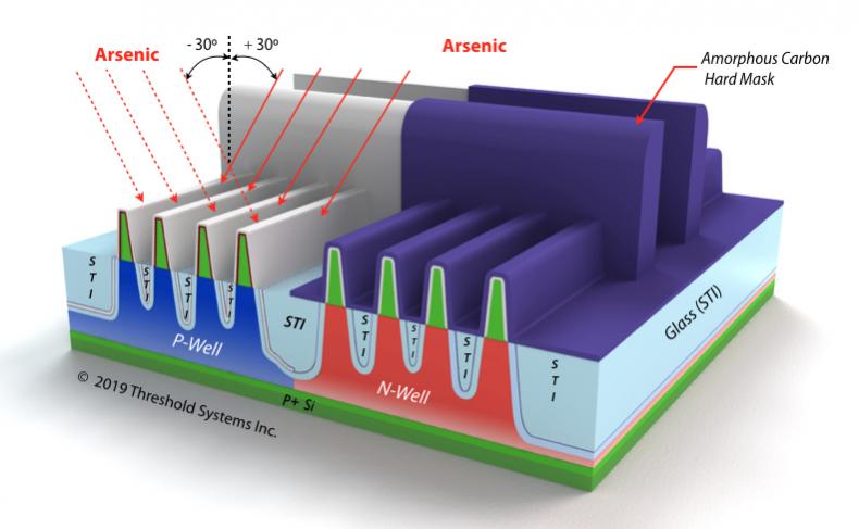
The problem of traditional FinFET Extension Implant doping concerns the awkward 3-dimensional structure of the fin. Because the Extension Implant defines the conductive electrical pathway between the Source/Drains and the undoped channel portion of the fin, it is essential that the fin be uniformly doped all three of its surfaces… Read More
The Evolution of the Extension Implant Part II
The use of hard masks instead of photoresist for the Extension implant is an effective way to optimize the amount of dopant that is retained along the fin sidewalls for those fins that border along photoresist edges (as discussed in Part 1 of this series).
However, hard masks do nothing to address the dominant problem driving steeper… Read More
The Evolution of the Extension Implant Part I
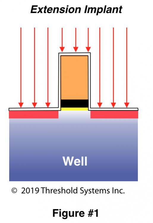
The 3D character of FinFET transistor structures pose a range of unique fabrication problems that can make it challenging to get these devices to yield. This is especially true for the all-important Extension implant that is put in place just prior to the nitride spacer formation.
The Extension implant is a central component of… Read More
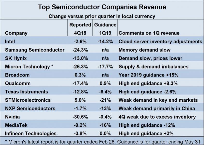
TSMC Q1 2019 Earnings Call Discussion!
It’s no coincidence that the TSMC Symposium is right after the Q1 earnings call. This will allow TSMC to talk more freely and they certainly will, my opinion. It is a very interesting time in the semiconductor industry and TSMC, being the bellwether, can tell us what will happen the rest of the year and give us some 2020 insights.… Read More
Samsung 5nm and TSMC 6nm Update
TSMC and Samsung continue to raise the competitive bar for FinFET foundry market share with dueling announcements this week. As I mentioned previously in the blog Semiconductor Foundry Landscape Update 2019, FinFETs are the market to watch with the coming onslaught of 5G and AI chips on the edge, in the cloud, and in our autonomous… Read More
Webinar: Addressing Multiphysics Challenges in 7nm FinFET Designs
EDA is big on growth through acquisition, being acquired many times throughout my career I know this by experience. In fact, we have a wiki that tracks EDA Mergers and Acquisitions and it is the most viewed wiki on SemiWiki.com with 101,918 views thus far.
In March of 2017 ANSYS acquired CLK Design Automation which did timing variation… Read More
Accelerating 5G Innovation and Reliability Through Simulation and Advanced FinFET Design
In an ANSYS seminar held at DesignCon 2019, Dr. Larry Williams, ANSYS Director of Technology, outlined how 5G design innovation can be accelerated through simulation. He posited that 5G will become a general-purpose technology that affects an entire economy, drastically alter societies and unleash a cascade of complementary… Read More
Where Circuit Simulation Model Files Come From
I started out my engineering career by doing transistor-level circuit design and we used a proprietary SPICE circuit simulator. One thing that I quickly realized was that the accuracy of my circuit simulations depended entirely on the model files and parasitics. Here we are 40 years later and the accuracy of SPICE circuit simulations… Read More


