You are currently viewing SemiWiki as a guest which gives you limited access to the site. To view blog comments and experience other SemiWiki features you must be a registered member. Registration is fast, simple, and absolutely free so please,
join our community today!
EDA is big on growth through acquisition, being acquired many times throughout my career I know this by experience. In fact, we have a wiki that tracks EDA Mergers and Acquisitions and it is the most viewed wiki on SemiWiki.com with 101,918 views thus far.
In March of 2017 ANSYS acquired CLK Design Automation which did timing variation… Read More
In an ANSYS seminar held at DesignCon 2019, Dr. Larry Williams, ANSYS Director of Technology, outlined how 5G design innovation can be accelerated through simulation. He posited that 5G will become a general-purpose technology that affects an entire economy, drastically alter societies and unleash a cascade of complementary… Read More
I started out my engineering career by doing transistor-level circuit design and we used a proprietary SPICE circuit simulator. One thing that I quickly realized was that the accuracy of my circuit simulations depended entirely on the model files and parasitics. Here we are 40 years later and the accuracy of SPICE circuit simulations… Read More
China has always been an intriguing semiconductor puzzle that very few companies have solved and now it is much more puzzling with the current political meandering. The GlobalFoundries vision of having foundries all over the world was very appealing to me back in 2009 and even more so today. Remember, China consumes more than half… Read More
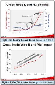
Technology scaling has made positive impacts on device performance, while creating challenges on the interconnects and the fidelity of its manufactured shapes. The process dimension scaling has significantly increased metal and via resistance for advanced nodes 7nm and onward, as shown in figures 1a,1b. Similar to a fancy… Read More
When TSMC’s annual Open Innovation Platform Exposition takes place, you know it will be time to hear about designs starting on the most advanced nodes. This year we were hearing about 7nm and 5nm. These newer nodes present even more challenges than previous nodes due to many factors. Regardless of what kind of design you are undertaking… Read More
GLOBALFOUNDRIES (GF) recently announced they were abandoning 7nm and focusing on “differentiated” foundry offerings in a move our own Dan Nenni described as a “pivot”, a description GF appears to have embraced. Last week GF held their annual Technology Conference and we got to hear more about the pivot from new CEO Tom Caulfield… Read More
As an IC designer I absolutely loved embarking on a new design project, starting with a fresh, blank slate, not having to use any legacy blocks. In the early 1980’s we really hadn’t given much thought to re-using semiconductor IP because each new project typically came with a new process node, so there was no IP even ready… Read More
The TSMC OIP event is next week and again it is packed with a wide range of technical presentations from TSMC, top semiconductor, EDA, and IP companies, plus long time TSMC partner and ASIC provider Open-Silicon, a SiFive Company. You can see the full agenda HERE.
AI is revolutionizing and transforming virtually every industry… Read More
TSMC is the leading foundry worldwide and they make a big splash each year at the DAC exhibit and conference, so I stopped by their theatre area during the presentation from IP vendor Moortec to see what’s new this year. Stephen Crosher was the presenter from Moortec and we had exchanged emails before, so this was the first time… Read More