You are currently viewing SemiWiki as a guest which gives you limited access to the site. To view blog comments and experience other SemiWiki features you must be a registered member. Registration is fast, simple, and absolutely free so please,
join our community today!
Stochastic defects in EUV lithography have been studied over the last few years. For years, the Poisson noise from the low photon density of EUV had been suspected [1,2]. EUV distinguishes itself from DUV lithography with secondary electrons functioning as intermediary agents in generating reactions in the resist. Therefore,… Read More
My name is Sagar, and I’ve been a long-time executive in the semiconductor manufacturing world — holding key positions at large multi-nationals, a leading semiconductor foundry, and partnering with many of the top-tier foundries and OSATs. Since “retiring”, I’ve also spent time advising and investing in start-ups through … Read More
Recently TechInsights analyzed a Bitcoin Miner chip fabbed at SMIC and declared SMIC has a 7nm process. There has been some debate as to whether the SMIC process is really 7nm and what it means if it is 7nm. I wanted to discuss the case for and against the process being 7nm, and what I think it means.
First off, I want to say I am not going … Read More
There is growing awareness that EUV lithography is actually an imaging technique that heavily depends on the distribution of secondary electrons in the resist layer [1-5]. The stochastic aspects should be traced not only to the discrete number of photons absorbed but also the electrons that are subsequently released. The electron… Read More
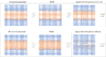
The 3nm node is projected to feature around a 22 nm metal pitch [1,2]. This poses some new challenges for the use of EUV lithography. Some challenges are different for the 0.33NA vs. 0.55NA systems.
0.33 NA
For 0.33 NA systems, 22 nm pitch can only be supported by illumination filling 4% of the pupil, well below the 20% lower limit for
…
Read More
-ASML reports strong quarter- Orders up 20% Qtr/Qtr
-Customers rush delivery which delays revenue recognition
-Chip makers need hard to get litho tools most of all
-Warning on concerns about consumer chip demand
Good numbers that are even better in reality
ASML reported revenues of Euro5.4B and EPS of Euro3.54. Most importantly… Read More
-If you can’t beat them, embargo them
-It has been reported US wants ASML to halt China DUV tools
-US obviously wants to kill, not just wound China chip biz
-Is this embargo the alternative to failed CHIPS act?
-Hard to say “do as I say, not as I do”- but US does anyway
First EUV ban now DUV ban? Are process & yield… Read More
At the 2022 SPIE Advanced Lithography Conference, ASML presented an update on EUV. I recently had a chance to go over the presentations with Mike Lercel of ASML. The following is a summary of our discussions.
0.33 NA
The 0.33 NA EUV systems are the production workhorse systems for leading edge lithography today. 0.33 NA systems are… Read More
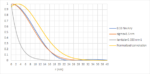
The next generation of EUV lithography systems are based on a numerical aperture (NA) of 0.55, a 67% increase from the current value of 0.33. It targets being able to print 16 nm pitch [1]. The High-NA systems are already expected to face complications from four issues: (1) reduced depth-of-focus requires thinner resists, which… Read More
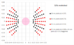
To the general public, EUV lithography’s resolution can be traced back to its short wavelengths (13.2-13.8 nm), but the true printed resolution has always been affected by the stochastic behavior of the electrons released by EUV absorption [1-5].
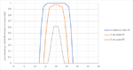
A 0.33 NA EUV system is expected to have a diffraction-limited point spread… Read More