You are currently viewing SemiWiki as a guest which gives you limited access to the site. To view blog comments and experience other SemiWiki features you must be a registered member. Registration is fast, simple, and absolutely free so please,
join our community today!
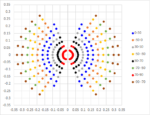
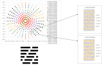
The stochastic nature of imaging has received a great deal of attention in the area of EUV lithography. The density of EUV photons reaching the wafer is low enough [1] that the natural variation in the number of photons arriving at a given location can give rise to a relatively large standard deviation.
In recent studies [2,3], it … Read More
EUV (Extreme UltraViolet) lithography has received attention within the semiconductor industry since its development inception in 1997 with the formation of the EUV LLC [1], and more recently, since the 7nm node began, with limited use by Samsung and TSMC being touted as key advantages [2, 3]. As with any key critical technology,
…
Read More
Economic damage-
China relationship damage will far outlast direct Covid19 logistics impact-
Economic damage could be huge but trade damage could be larger with more specific impact on chips-
A long build up to a China trade nuclear winter, the “drum-beat of war”
When we started talking about a potential chip trade… Read More
Covid issues create “lumpy” quarters due to delays
Orders & demand remain solid and strong
2020 Year financials intact so far but ignore Qtrs
Taking prudent actions- no buybacks or guidance
As expected, Covid impacts both shipments & supply chain, ignore the near term lumpiness…
ASML reported revenues… Read More
I couldn’t attend the SPIE Advanced Lithography Conference this year for personal reasons, but last week Mike Lercel of ASML was nice enough to walk me through the major ASML presentations from the conference.
Introduction
In late 2018, Samsung and TSMC introduced 7nm foundry logic processes with 5 to 7 EUV layers, throughout … Read More
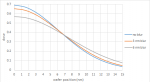
State-of-the-art chips will always include some portions which are memory arrays, which also happen to be the densest portions of the chip. Arrayed features are the main targets for lithography evaluation, as the feature pitch is well-defined, and is directly linked to the cost scaling (more features per wafer) from generation… Read More
Our friends at Threshold Systems have a new ONLINE class that may be of interest to you. It’s an updated version of the Advanced CMOS Technology class held last February. This is normally a classroom affair but to accommodate the recent COVID-19 travel restrictions it is being offered virtually.
As part of the previous class we did… Read More
As any semiconductor process advances to the next generation or “node”, a sticky point is how to achieve the required higher resolution. As noted in another article [1], multipatterning (the required use of repeated patterning steps for a particular feature) has been practiced already for many years, and many have… Read More
EUV lithography is widely perceived to be the obvious choice to replace DUV lithography due to the shorter wavelength(s) used. However, there’s a devil in the details, or a catch if you will.
Electrons have the last word
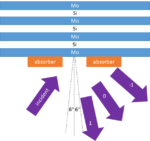
The resist exposure is completed by the release of electrons following the absorption of the EUV photon.… Read More
Extreme ultraviolet (EUV) lithography targets sub-20 nm resolution using a wavelength range of ~13.3-13.7 nm (with some light including DUV outside this band as well) and a reflective ring-field optics system. ASML has been refining the EUV tool platform, starting with the NXE:3300B, the very first platform with a numerical
…
Read More