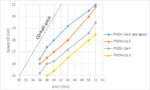
Application-Specific Lithography: The 5nm 6-Track Cell

Application-Specific Lithography: The 5nm 6-Track Cell
by Fred Chen on 07-05-2020 at 10:00 am

Application Specific Lithography The 5nm 6 Track Cell

The 5nm foundry (e.g., TSMC) node may see the introduction of 6-track cells (two double-width rails plus four minimum-width dense lines) with a minimum metal pitch in the neighborhood of 30 nm. IMEC had studied a representative case as its ‘7nm’ case [1]. TSMC had some published 5nm test structures which looked like… Read More


The Stochastic Impact of Defocus in EUV Lithography

The Stochastic Impact of Defocus in EUV Lithography
by Fred Chen on 06-28-2020 at 6:00 am

The Stochastic Impact of Defocus in EUV Lithography

The stochastic nature of imaging has received a great deal of attention in the area of EUV lithography. The density of EUV photons reaching the wafer is low enough [1] that the natural variation in the number of photons arriving at a given location can give rise to a relatively large standard deviation.

In recent studies [2,3], it … Read More


The Uncertain Phase Shifts of EUV Masks

The Uncertain Phase Shifts of EUV Masks
by Fred Chen on 05-13-2020 at 10:00 am

The Uncertain Phase Shifts of EUV Masks

EUV (Extreme UltraViolet) lithography has received attention within the semiconductor industry since its development inception in 1997 with the formation of the EUV LLC [1], and more recently, since the 7nm node began, with limited use by Samsung and TSMC being touted as key advantages [2, 3]. As with any key critical technology,

Read More

Covid Created Collateral China Crisis

Covid Created Collateral China Crisis
by Robert Maire on 05-03-2020 at 6:00 am

China US Trade Agreement 2020

Economic damage-
China relationship damage will far outlast direct Covid19 logistics impact-
Economic damage could be huge but trade damage could be larger with more specific impact on chips-

A long build up to a China trade nuclear winter, the “drum-beat of war”
When we started talking about a potential chip trade… Read More


ASML A Scenario More Lumpy While Demand and Tech Remain Solid Despite Covid Delays

ASML A Scenario More Lumpy While Demand and Tech Remain Solid Despite Covid Delays
by Robert Maire on 04-22-2020 at 2:00 pm

ASML SemiWiki 2020

Covid issues create “lumpy” quarters due to delays
Orders & demand remain solid and strong
2020 Year financials intact so far but ignore Qtrs
Taking prudent actions- no buybacks or guidance

As expected, Covid impacts both shipments & supply chain, ignore the near term lumpiness…
ASML reported revenues… Read More


SPIE 2020 – ASML EUV and Inspection Update

SPIE 2020 – ASML EUV and Inspection Update
by Scotten Jones on 04-20-2020 at 10:00 am

0.33 NA EUV systems for HVM Ron Schuurhuis Page 02

I couldn’t attend the SPIE Advanced Lithography Conference this year for personal reasons, but last week Mike Lercel of ASML was nice enough to walk me through the major ASML presentations from the conference.

Introduction
In late 2018, Samsung and TSMC introduced 7nm foundry logic processes with 5 to 7 EUV layers, throughout … Read More


Lithography Resolution Limits – Arrayed Features

Lithography Resolution Limits – Arrayed Features
by Fred Chen on 04-17-2020 at 6:00 am

Lithography Resolution Limits Arrayed Features

State-of-the-art chips will always include some portions which are memory arrays, which also happen to be the densest portions of the chip. Arrayed features are the main targets for lithography evaluation, as the feature pitch is well-defined, and is directly linked to the cost scaling (more features per wafer) from generation… Read More


Online Class: Advanced CMOS Technology 2020 (The 10/7/5 NM Nodes)

Online Class: Advanced CMOS Technology 2020 (The 10/7/5 NM Nodes)
by Daniel Nenni on 04-12-2020 at 9:00 am

3D Finet Model

Our friends at Threshold Systems have a new ONLINE class that may be of interest to you. It’s an updated version of the Advanced CMOS Technology class held last February. This is normally a classroom affair but to accommodate the recent COVID-19 travel restrictions it is being offered virtually.

As part of the previous class we did… Read More


Lithography Resolution Limits: Paired Features

Lithography Resolution Limits: Paired Features
by Fred Chen on 04-07-2020 at 10:00 am

Lithography Resolution Limits Paired Features

As any semiconductor process advances to the next generation or “node”, a sticky point is how to achieve the required higher resolution. As noted in another article [1], multipatterning (the required use of repeated patterning steps for a particular feature) has been practiced already for many years, and many have… Read More


Low Energy Electrons Set the Limits for EUV Lithography

Low Energy Electrons Set the Limits for EUV Lithography
by Fred Chen on 03-25-2020 at 6:00 am

Low Energy Electrons Set the Limits for EUV Lithography

EUV lithography is widely perceived to be the obvious choice to replace DUV lithography due to the shorter wavelength(s) used. However, there’s a devil in the details, or a catch if you will.

Electrons have the last word
The resist exposure is completed by the release of electrons following the absorption of the EUV photon.… Read More