You are currently viewing SemiWiki as a guest which gives you limited access to the site. To view blog comments and experience other SemiWiki features you must be a registered member. Registration is fast, simple, and absolutely free so please,
join our community today!
The resolution of EUV lithography is commonly expected to benefit from the shorter wavelengths (13.2-13.8 nm) but in actuality the printing process needs to include Pde the consideration of the lower energy electrons released by the absorption of EUV photons. The EUV photon energy itself has a nominal energy range of 90-94 eV,… Read More
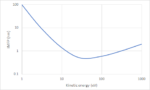
In spite of increasing usage of EUV lithography, stochastic defects have not gone away. What’s becoming clearer is that EUV doses must be managed to minimize the impact from such defects. The 2022 edition of the International Roadmap for Devices and Systems has updated its Lithography portion [1]. An upward trend with decreasing… Read More
The 3nm node is projected to feature around a 22 nm metal pitch [1,2]. This poses some new challenges for the use of EUV lithography. Some challenges are different for the 0.33NA vs. 0.55NA systems.
0.33 NA
For 0.33 NA systems, 22 nm pitch can only be supported by illumination filling 4% of the pupil, well below the 20% lower limit for
…
Read More
As a consequence of having a ~13.5 nm wavelength, EUV photons transfer ~90% of their energy to ionized photoelectrons. Thus, EUV lithography is fundamentally mostly EUV photoelectron lithography. The actual resolution becomes dependent on photoelectron trajectories.
Photoelectron trajectories in EUV lithography were… Read More
The list of possible stochastic patterning issues for EUV lithography keeps growing longer: CD variation, edge roughness, placement error, defects [1]. The origins of stochastic behavior are now well-known. For a given EUV photon flux into the resist, a limited fraction are absorbed. Since the absorption is less than 5% affected… Read More
Stochastic defects continue to draw attention in the area of EUV lithography. It is now widely recognized that stochastic issues not only come from photon shot noise due to low (absorbed) EUV photon density, but also the resist material and process factors [1-4].
It stands to reason that resist absorption of EUV light, which is … Read More
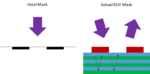
As EUV lithography is being targeted towards pitches of 30 nm or less, fundamental differences from conventional DUV lithography become more and more obvious. A big difference is in the mask use. Unlike other photolithography masks, EUV masks are absorber patterns on a reflective multilayer rather than a transparent substrate.… Read More
In previous articles, I had looked at EUV stochastic behavior [1-2], primarily in terms of the low photon density resulting in shot noise, described by the Poisson distribution [3]. The role of blur to help combat the randomness of EUV photon absorption and secondary electron generation and migration was also recently considered… Read More
Recent advances in EUV lithography have largely focused on “low-k1” imaging, i.e., features with pitches less than the wavelength divided by the numerical aperture (k1<0.5). With a nominal wavelength of 13.5 nm and a numerical aperture of 0.33, this means sub-40 nm pitches. It is naturally expected that larger… Read More
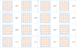
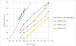
Ongoing investigations of EUV stochastics [1-3] have allowed us to map combinations of critical dimension (CD) and pitch which are expected to pose a severe risk of stochastic defects impacting the use of EUV lithography. Figure 1 shows a typical set of contours of fixed PNOK (i.e., the probability of a feature being Not OK due… Read More