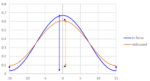
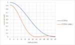
Conventionally, the resolution limit of a lithography system with wavelength l and numerical aperture NA is given by half-pitch = 0.25 wavelength/NA. With the use of EUV lithography, however, electron blur needs to be added [1]. The impact of this blur is to reduce the contrast [2]. Blur reduces the modulation amplitude by a factor… Read More

Tag: euv lithography
Stochastic Pupil Fill in EUV Lithography

Pupil fill tradeoff again
EUV lithography continues to be plagued by its stochastic nature.
This stochastic nature is most clearly portrayed by the random fluctuation of the absorbed photon number at a given location. For example, consider an absorbed dose of 10 mJ/cm2 amounts to 6.8 photons of energy 92 eV absorbed in a square … Read More
Why NA is Not Relevant to Resolution in EUV Lithography
The latest significant development in EUV lithography technology is the arrival of High-NA systems. Theoretically, by increasing the numerical aperture, or NA, from 0.33 to 0.55, the absolute minimum half-pitch is reduced by 40%, from 10 nm to 6 nm. However, for EUV systems, we need to recognize that the EUV light (consisting … Read More
Non-EUV Exposures in EUV Lithography Systems Provide the Floor for Stochastic Defects in EUV Lithography
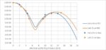
EUV lithography is a complicated process with many factors affecting the production of the final image. The EUV light itself doesn’t directly generate the images, but acts through secondary electrons which are released as a result of ionization by incoming EUV photons. Consequently, we need to be aware of the fluctuations… Read More
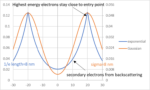
Predicting Stochastic Defectivity from Intel’s EUV Resist Electron Scattering Model
The release and scattering of photoelectrons and secondary electrons in EUV resists has often been glossed over in most studies in EUV lithography, despite being a fundamental factor in the image formation. Fortunately, Intel has provided us with a laboriously simulated electron release and scattering model, using the GEANT4… Read More
The Significance of Point Spread Functions with Stochastic Behavior in Electron-Beam Lithography
Electron beam lithography is commercially used to directly write submicron patterns onto advanced node masks. With the advent of EUV masks and nanometer-scale NIL (nanoimprint lithography), multi-beam writers are now being used, compensating the ultralow throughput of a single high-resolution electron beam with the use… Read More
Advancing Semiconductor Processes with Novel Extreme UV Photoresist Materials

Introduction
The ever-growing demand for faster, smaller, and more efficient electronic devices has fueled the semiconductor industry’s relentless pursuit of innovation. One crucial technology at the heart of semiconductor manufacturing is Extreme Ultraviolet Lithography (EUVL) to achieve smaller feature sizes… Read More
Lithography Resolution Limits: The Point Spread Function
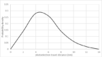
The point spread function is the basic metric defining the resolution of an optical system [1]. A focused spot will have a diameter defined by the Airy disk [2], which is itself a part of the diffraction pattern, based on a Bessel function of the 1st kind and 1st order J1(x), with x being a normalized coordinate defined by pi*radius/(0.5… Read More
Multiple Monopole Exposures: The Correct Way to Tame Aberrations in EUV Lithography?
For a leading-edge lithography technology, EUV (extreme ultraviolet) lithography is still plagued by some fundamental issues. While stochastically occurring defects probably have been the most often discussed, other issues, such as image shifts and fading [1-5], are an intrinsic part of using reflective EUV optics. However,… Read More
Secondary Electron Blur Randomness as the Origin of EUV Stochastic Defects

Stochastic defects in EUV lithography have been studied over the last few years. For years, the Poisson noise from the low photon density of EUV had been suspected [1,2]. EUV distinguishes itself from DUV lithography with secondary electrons functioning as intermediary agents in generating reactions in the resist. Therefore,… Read More