For Halloween this week we thought it would be appropriate to talk about things that strike fear into the hearts of semiconductor makers and process engineers toiling away in fabs. Do I want to do multi-patterning with the huge increase in complexity, number of steps, masks and tools or do I want to do EUV with unproven tools, unproven… Read More
Tag: 7nm
Silicon Creations talks about 7nm IP Verification for AMS Circuits
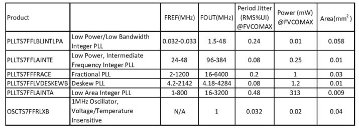
Designing at 7nm is a big deal because of the costs to make masks and then produce silicon that yields at an acceptable level, and Silicon Creations is one company that has the experience in designing AMS IP like: PLL, Serializer-Deserializer, IOs, Oscillators. Why design at 7nm? Lots of reasons – lower power, higher speeds,… Read More
GLOBALFOUNDRIES RF Leadership
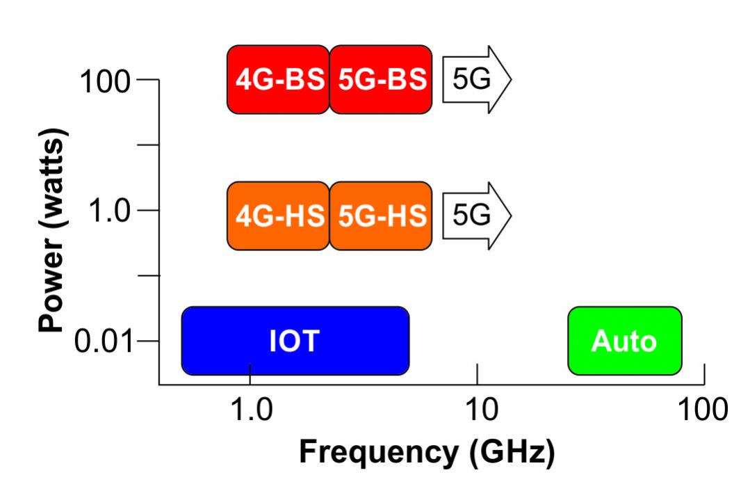
“Mobile is the largest platform ever built by humanity”, Christiano Amon, Executive Vice President, Qualcomm Technologies, Inc. and President, Qualcomm CDMA Technologies speaking at the GLOBALFOUNDRIES Technologies Conference (GTC) 2017.… Read More
IEDM 2017 Preview
The 63rd annual IEDM (International Electron Devices Meeting) will be held December 2nd through 6th in San Francisco. In my opinion IEDM is one of, if not the premier conference on leading edge semiconductor technology. I will be attending the conference again this year and providing coverage for SemiWiki. As a member of the press… Read More
TSMC Teamwork Translates to Technical Triumph
Most people think that designing successful high speed analog circuits requires a mixture of magic, skill and lots of hard work. While this might be true, in reality it also requires a large dose of collaboration among each of the members of the design, tool and fabrication panoply. This point was recently made abundantly clear … Read More
GLOBALFOUNDRIES is Hitting on all Cylinders
On September 20th GLOBALFOUNDRIES (GF) held their annual technology conference. The conference presented an opportunity to hear the latest on the fascinating journey GF has been on.… Read More
SEMICON West – EUV Readiness Update
At the imec technology forum held at SEMICON West, Martin Van Den Brink, President and CTO of ASML presented on the latest developments on EUV. I also had an opportunity to sit down with Mike Lercel, ASML Director of Strategic Marketing for an interview.… Read More
SEMICON West – Advanced Interconnect Challenges
At SEMICON West I attended the imec technology forum where Zsolt Tokei presented “How to Solve the BEOL RC Dilemma” and the SEMICON Economics of Density Scaling session where Larry Clevenger of IBM presented “Interconnect Scaling Strategic for Advanced Semiconductor Nodes”. I also had the opportunity… Read More
Standard Node Trend
I have previously published analysis’ converting leading edge logic processes to “standard nodes” and comparing standard nodes by company and time. Recently updated details on the 7nm process node have become available and in this article, I will revisit the standard node calculations and trends.… Read More
Machine Learning in EDA Flows – Solido DAC Panel
At DAC this year you could learn a lot about hardware design for AI or Machine Learning (ML) applications. We are all familiar with the massively parallel hardware being developed for autonomous vehicles, cloud computing, search engines and the like. This includes, for instance, hardware from Nvidia and others that enable ML … Read More


