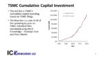
You are currently viewing SemiWiki as a guest which gives you limited access to the site. To view blog comments and experience other SemiWiki features you must be a registered member. Registration is fast, simple, and absolutely free so please,
join our community today!
I have seen several articles recently discussing foundry wafer selling prices for leading edge wafers, these articles all quote estimates from a paper by the Center for Security and Emerging Technology (CSET). The paper is available here.
My company IC Knowledge LLC is the world leader in cost and price modeling of semiconductors… Read More
TSMC’s Open Innovation Platform’s main objective is to create and promote partnership for producing chips. This year’s OIP event included a presentation on the joint efforts of Silicon Creations, Mentor, a Siemens business and TSMC to produce essential PLL IP for 5nm and 3nm designs. The relentless push for smaller geometries… Read More
For the 10nm – 5nm nodes, the leading-edge foundries are designing cells which utilize 6 or 7 metal tracks, entailing a wide metal line for every 4 or 5 minimum width lines, respectively (Figure 1).
Figure 1. Left: a 7-track cell. Right: a 6-track cell.
This is a fundamental vulnerability for lithography, as defocus can change… Read More
At SEMICON West, Applied Materials announced a new selective gap fill tool to address the growing resistance issues in interconnect at small dimensions. I had the opportunity to discuss this new tool and the applications for it with Zhebo Chen global product manager in the Metal Deposition Products group at Applied Materials.… Read More
The 2020 VLSI Technology Symposium was held as a virtual conference from June 14th through June 19th. At the symposium Imec gave an interesting paper on Buried Power Rails (BPR) and I had a chance to interview one of the authors, Anshul Gupta.
As logic devices continue to scale down metal pitch is reaching a limit. Imec defines a pitch… Read More
The 5nm foundry (e.g., TSMC) node may see the introduction of 6-track cells (two double-width rails plus four minimum-width dense lines) with a minimum metal pitch in the neighborhood of 30 nm. IMEC had studied a representative case as its ‘7nm’ case [1]. TSMC had some published 5nm test structures which looked like… Read More
TSMC pushing out equipment purchases
Covid/China trickles down to chip industry
SIA and SEMI ask for financial/govt help to keep up
The beginning of another down cycle?
We have heard from a number of sources that TSMC has started to push out equipment orders as concerns grow about the second half of the year.
Right now is the most logical… Read More
On May 15th TSMC “announced its intention to build and operate an advanced semiconductor fab in the United States with the mutual understanding and commitment to support from the U.S. federal government and the State of Arizona.”
The fab will run TSMC’s 5nm technology and have a capacity of 20,000 wafers per month (wpm). Construction… Read More
Recently Seeking Alpha published an article “Taiwan Semiconductor Manufacturing Company Losing Its Process Leadership To Intel” and Dan Nenni (SemiWiki founder) asked me to take a look at the article and do my own analysis. This is a subject I have followed and published on for many years.
Before I dig into specific process density… Read More
I couldn’t attend the SPIE Advanced Lithography Conference this year for personal reasons, but last week Mike Lercel of ASML was nice enough to walk me through the major ASML presentations from the conference.
Introduction
In late 2018, Samsung and TSMC introduced 7nm foundry logic processes with 5 to 7 EUV layers, throughout … Read More