 I attended a panel session followed by a party during Semicon to celebrate Soitec’s 20th birthday. Officially it was titled An Insider’s Look at the Future of Mobile Technologies. But in reality it was a look at the future possibilities for SOI.
Silicon on Insulator (SOI) has been a sort of bastard child of semiconductor. Almost all foundry work (TSMC, GF etc) and Intel in particular has been bulk CMOS. But both IBM and AMD have used SOI for high performance microprocessors. The drawback of SOI is that it is more expensive than bulk to manufacture.
When FinFETs were first invented, it was an SOI-based technology. It is much easier to form the gate over the fin when the substrate stops the etch. It also only had gate on the sides of the fin and not over the top. But TSMC worked out how to put the gate completely around the fin, and Samsung worked out how to manufacture it on bulk technology. The highest profile FinFET proponent is Intel with its tri-gate process, which is bulk although beyond 14nm apparently they are looking at SOI. TSMC is also going FinFET although less aggressively than Intel.

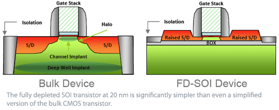
But ST microelectronics is taking the SOI approach and building its advanced processes using fully-depleted SOI (FDSOI). As I explained in a blog earlier this year, as we go below 28nm you have to have the whole channel well-controlled by the gate and that means the channel must be very thin. One way is to build it vertically (the FinFET) and the other way is to make the gate on an insulator so it is still a 2D structure but the channel really is thin. ST were one of the participants on the panel session.
The panelists were:
- Ron Moore of ARM
- Subramani Kengeri of GlobalFoundries
- Gary Patton of IBM
- Horacio Mendez of SOI Industry Consortium
- Steve Longoria of Soitec
- Philippe Margashack of STM
- Chenming Hu of UC Berkeley
The panel session was a bit like that party game in which you get eliminated if you say “yes” or “no,” except this time you were not allowed to say Intel…even when clearly talking about them. In the end, Dr Chenming Hu, the inventor of the FinFET, gave in and said the dirty word towards the end of the panel. But I expect he consults to them on FinFETs so I guess he had a free pass.
Clearly SOI has a strong future going forward, with ST committed to it, Global planning on using SOI as well as bulk and, as we move down the process nodes (if we can get an economically viable lithography working) it seems to make some things easier especially in the foundry business where there is a bigger separation between process and design.
Share this post via:


Comments
0 Replies to “Silicon on Insulator (SOI)”
You must register or log in to view/post comments.