
In my career in semiconductor industry, I can recall, in the beginning there was emphasis on design completion with automation as fast as possible. The primary considerations were area and speed of completion of a semiconductor design. Today, with unprecedented increase in multiple functions on the same chip and density of the design, power has become critical to the design. And excessive power consumption has given rise to a fourth parameter, temperature to consider at the beginning of the design; it’s no longer uniform across the die. Further, a thinner die is losing its heat spreading capability. Considering the kind of high heat generation inside the chips now a day, temperature has become a critical aspect to look at, not only its generation due to power consumption, but also separately by taking into account the planning of temperature distribution and diffusion, thermal properties of materials, and collaborating between mechanical and electrical design flow. In case of stacked dies in 3DICs, it’s essential that proper mechanisms are planned to get the heat out of the stack. The placement of TSVs (Through Silicon Vias) near high power regions can significantly improve the overall thermal performance of a 3DIC.
Mentor Graphicswith its experience through the use of its tools in TSMC’sCoWoS Reference Flow for design, verification, thermal and test solutions, and a study with experts have proposed key guidelines for thermal management which can be followed through a design flow from start of the design.
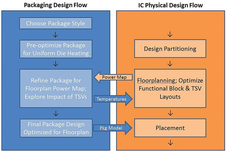
It’s important to consider the chip-package co-design, starting with the package construction (which may be mounted on a PCB) in the thermal model such that the effect of heat spreading in the board and into any heat sink (if planned) are accounted for in predicting the package temperature distribution. It requires a complete CFD (Computational Fluid Dynamics) simulation to study and predict the thermal interaction of the package with its environment. In the beginning of a design, a 3D thermal conduction model for the whole package as per the number of dies and budgeted power for each die can be planned very effectively and temperature data back-annotated to the IC design flow.
Explore the package design space with different package materials, die arrangements, package design, size and options and so on. The temperature influencing parameters such as TSV layout, interposer shape, size and material, glue layers, cooling solutions, stack design etc. can be studied at this stage.
The temperature-dependent thermal properties must be included. Mentor’s FloTHERM has a material library which includes all kinds of materials with their thermal properties such as temperature-dependent thermal conductivity, specific heat capacity and material density to accurately predict hot spots on a die.
The die surface treatment should be refined by including a 3D representation of the active layers (consisting of metal wires separated by dielectric materials) of the die approximated to an isotropic block within the thickness of one mesh cell in the package-level model.
It’s interesting to note that by this time the bulk top-level planning is done to estimate the average die temperature and temperature variation for each die. This information of temperature can be back-annotated before floorplanning that can help the IC design team to effectively partition and floorplan the design appropriately at the start of the design process.

Now it’s time to refine the package further with input from the IC design team; the power map after floorplanning can be imported into the thermal model of the package. FloTHERM has a Die SmartPart that allows power to be read in as CSV file automatically and the thermal simulation model can quickly indicate where TSVs can be introduced to improve the thermal performance, or where design changes are needed such as to ensure a few functional blocks to operate at similar temperatures to eliminate timing issues. The functional blocks can be moved keeping their relative positions intact and optimizing the white spaces for insertion of TSVs. By using FloTHERM, an assessment of the impact of TSVs on the die hot spots can be easily done. Knowing the TSV size and pitch, which scale with die thickness, blocks of higher through-plane thermal conductivity can be superimposed over the die thickness in the white spaces in FloTHERM, to locally override the properties of silicon.
With the progress of the floorplanning and detailed thermal interaction between die, the power map for the die becomes much more detailed, thus making the IC design flow temperature aware. The thermal map created from power map (generated by power analysis tools) can be used for thermal design and checking against thermal constraints.
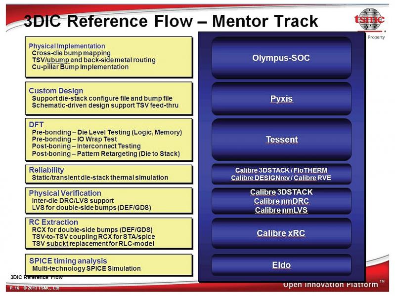
The FloTHERM is embedded into Mentor’s Calibre suite which enabled the creation of TSMC reference flow for thermal analysis based on FloTHERM and Calibre DESIGNrev and RVE, an industry standard physical verification result viewing environment. The automatic gridding (using localized grid in critical areas) built into this system enables very efficient, fast and accurate thermal simulation on dies and interposers of 3DIC.
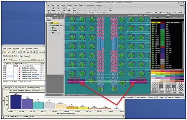
The thermal results can be displayed as histogram in Calibre RVE and the hot spots highlighted in Calibre DESIGNrev. In case of transient analysis, EZwave can be used to display temperature vs. time graph.
A 3DIC thermal model can be created to allow the 3DIC package to be imported into a larger system for further thermal simulation at the system level. A detailed study of the chip-package thermal co-design process can be found in a whitepaper at the Mentor website.
More Articles by Pawan Fangaria…..
Share this post via:


Comments
0 Replies to “Temperature – The Fourth Aspect to Look at in SoC Design”
You must register or log in to view/post comments.