While there is a lot of excitement around the semiconductor shortage narrative and the fabs all being full, both 200mm and 300mm, there is one big plot hole and that is the FinFET era.
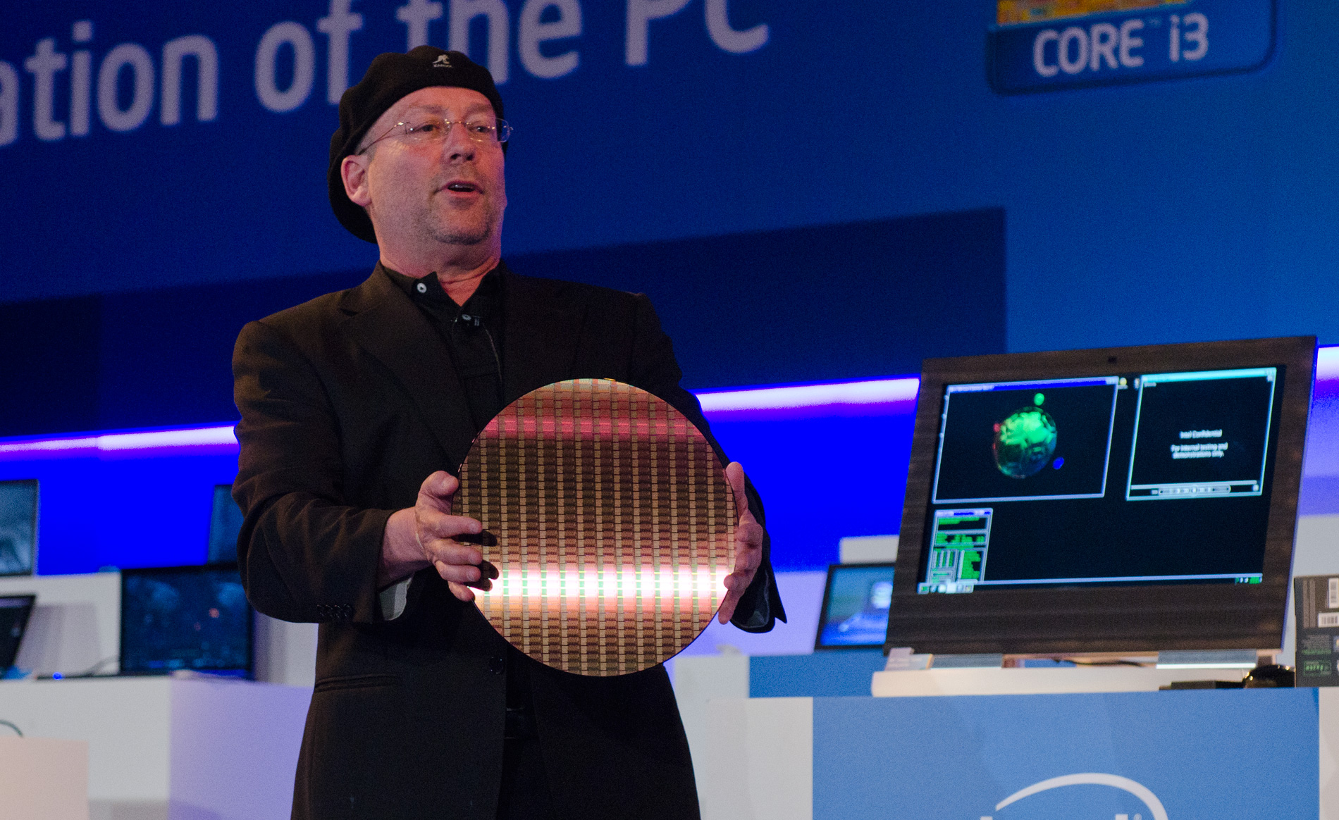
Intel ushered in the FinFET era only to lose FinFET dominance to the foundries shortly thereafter. In 2009 Intel brought out a 22nm FinFET wafer at the Intel Developers Conference and announced that chips would be available in the second half of 2011. True to their word, the first FinFET chip (code named Ivey Bridge) was officially announced in May of 2011. I remember being shocked that the details were not leaked prior to the announcement. Intel 22nm was truly a transformative process technology, absolutely.

Intel followed 22nm with 14nm which was late and yield challenged (double patterning FinFETs) which allowed the foundries to catch up (TSMC 16nm and Samsung 14nm). Samsung did a very nice job at 14nm and won quite a bit of business including a slice of the Apple iPhone pie.
TSMC took a different approach to FinFETs. After mastering double patterning on 20nm, TSMC added in FinFETs and called it 16nm. The density was less than Intel 14nm thus the name difference. Samsung 14nm was a similar density as TSMC 16nm but Samsung took the low road and pretended they were competitive with Intel. And that is why process nodes are now marketing terms, my opinion.
This all started what I call the Apple half step process development methodology. TSMC would release a new process version without fail for Apple every year. Prior to that processes were like fine wine, not to be uncorked until they were Moore’s Law ready. The half steps continued with TSMC adding partial EUV to a process already in HVM (7nm) then adding more EUV layers to 5nm and 3nm in a very controlled manner that allowed for superior yield learning and record breaking process ramps.
Intel 14nm is also when the “Intel versus TSMC” marketing battle started. Intel insisted that TSMC 20nm was a failure since it did not include FinFETs and foundries could not follow Intel since they were an IDM and TSMC was just a foundry with no in-house design experience.
As we now know, Intel was wrong on so many levels. First and foremost the foundry business is a services business with a massive partnership ecosystem which puts IDM foundries at a distinct disadvantage. It will be interesting to see how the Intel IDM 2.0 strategy pans out but most guesses are that it will fail harder than the previous attempt, but I digress.
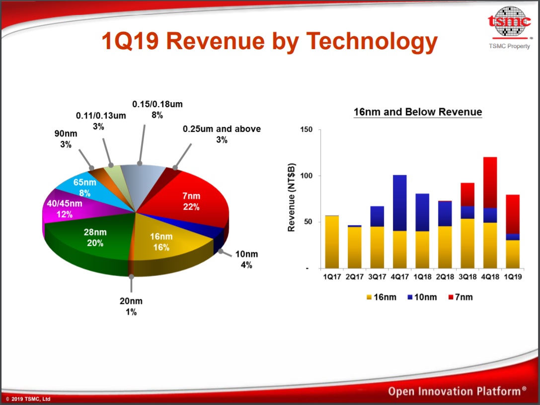
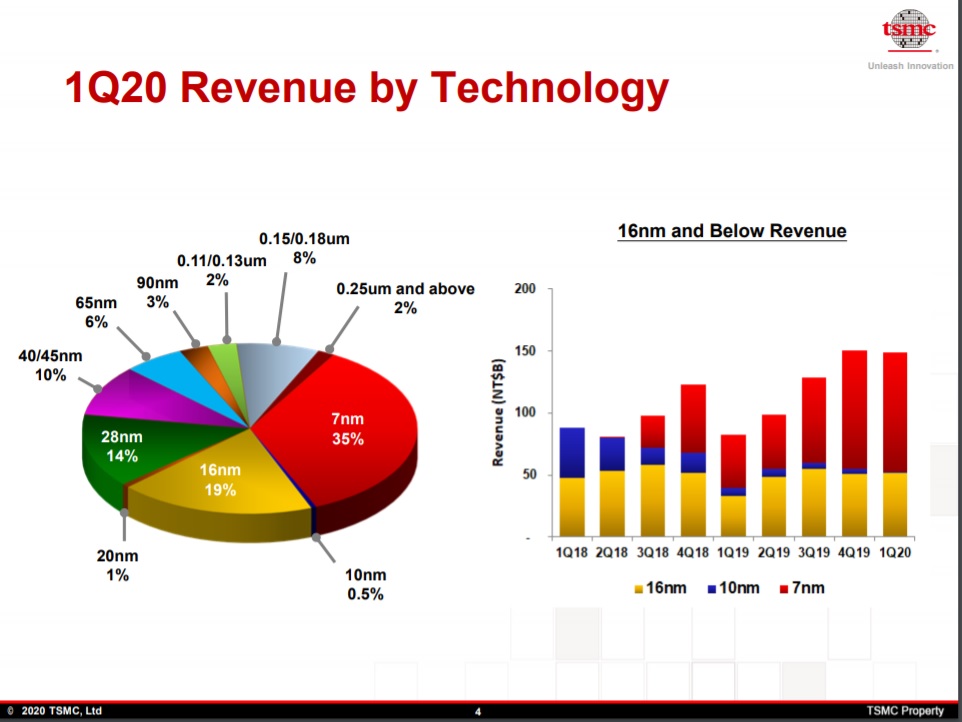
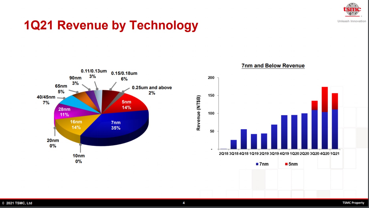
Now let’s take a quick look at the TSMC FinFET process revenue steps starting with Q1 2019 and the Q1s that have followed:


In Q1 2019 FinFETs accounted for 42% of TSMC revenue. In Q1 2020 it was 54.5% In Q1 2021 it was a whopping 63% and you can expect this aggressive ramp to continue for three reasons:
(1) TSMC protects their FinFET processes recipes so there is no second sourcing.
(2) FinFETs mean more performance at less power and less power is critical given the environmental challenges the world is facing.
(3) TSMC is building massive amounts of FinFET capacity ($100B 3 year CAPEX) and with the current semiconductor shortage narrative that is a VERY big deal.
Bottom line: TSMC is pushing their 500+ customers hard into the FinFET era and that will again change the foundry landscape.
The trillion dollar question is: What will happen to the mature (non-FinFET) nodes in the not too distant future? And more importantly, what will happen to the foundries that did not make the jump to FinFETs?
Share this post via:


Comments
11 Replies to “TSMC and the FinFET Era!”
You must register or log in to view/post comments.