TSMC as Pure Play Wafer Foundry
TSMC started its wafer foundry business more than 30 years ago. Visionary management and creative engineering teams developed leading-edge process technologies and their reputation as trusted source for high-volume production. TSMC also recognized very early the importance of building an ecosystem – to complement the company’s own strengths. Their Open Innovation Platform (OIP) attracted many EDA and IP partners to contribute to TSMC’s success, all following Moore’s Law, to 3 nm at this time, to serve very high-volume applications.
Markets need Advanced IC Packaging technologies
For many other applications Moore’s Law is no longer cost-effective, especially not for integration of heterogeneous functions. “Moore than Moore” technologies, like Multi-chip modules (MCMs) and System in Package (SiP) have become alternatives for integrating large amounts of logic and memory, analog, MEMS, etc. into (sub)system solutions. However, these methodologies were and still are very customer specific and incur significant development time and cost.
In response to market needs for new multi-die IC packaging solutions, TSMC has developed, in cooperation with OIP partners, advanced IC packaging technologies to offer economical solutions for More than Moore integration.
TSMC as supplier of Advanced IC Packaging solutions
In 2012 TSMC introduced, together with Xilinx, the by far largest FPGA available at that time, comprised of four identical 28 nm FPGA slices, mounted side-by-side, on a silicon interposer. They also developed through-silicon-vias (TSVs), micro-bumps and re-distribution-layers (RDLs) to interconnect these building blocks. Based on its construction, TSMC named this IC packaging solution Chip-on-Wafer-on-Substrate (CoWoS). This building blocks-based and EDA-supported packaging technology has become the de-facto industry standard for high-performance and high-power designs. Interposers, up to three stepper fields large, allow combining multiple die, die-stacks and passives, side by side, interconnected with sub-micron RDLs. Most common applications today are combinations of a CPU/GPU/TPU with one or more high bandwidth memories (HBMs).
In 2017 TSMC announced the Integrated FanOut technology (InFO). It uses, instead of the silicon interposer in CoWoS, a polyamide film, reducing unit cost and package height, both important success criteria for mobile applications. TSMC has already shipped tens of millions of InFO designs for use in smartphones.
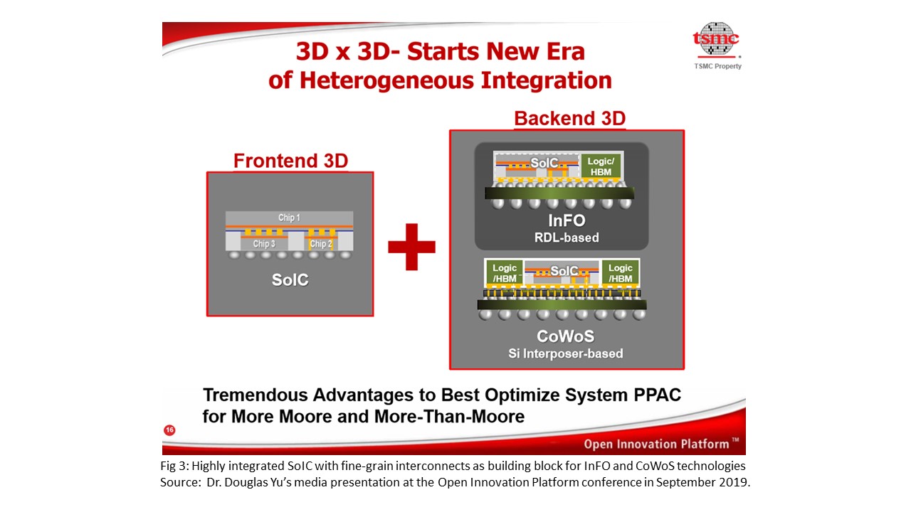
In 2019 TSMC introduced the System on Integrated Chip (SoIC) technology. Using front-end (wafer-fab) equipment, TSMC can align very accurately, then compression-bond designs with many narrowly pitched copper pads, to further minimize form-factor, interconnect capacitance and power.

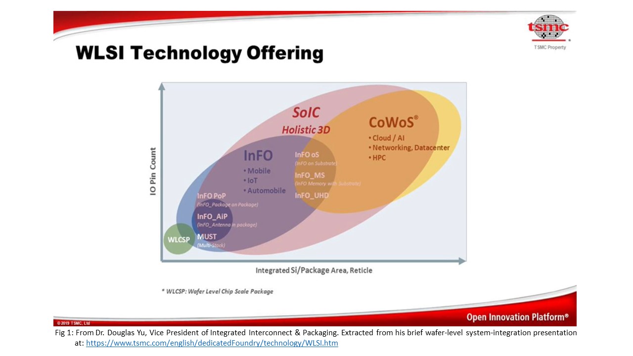
Figure 1 shows that CoWoS technology is targeting Cloud, AI, Networking, Datacenters and other high-performance and high-power computing applications.
InFO serves some of these and a broad range of other, typically more cost-sensitive and lower power markets.
SoIC technology offers multi-die building blocks for integration in CoWoS and/or InFO designs. – see Figure 2.

SoIC technology benefits
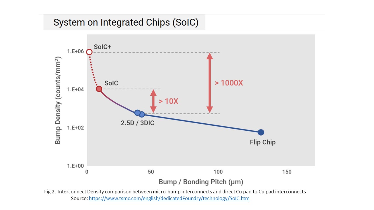
TSMC’s latest innovation, the SoIC technology is a very powerful way for stacking multiple dice into a “3D building block” (a.k.a. “3D-Chiplet”). Today SoICs enable about 10,000 interconnects per mm2 between vertically stacked dice. Development efforts towards 1 Million interconnects per mm2 are ongoing. 3D-IC enthusiasts, including myself, have been looking, for an IC packaging methodology that enables such fine-grain interconnects, further reduces form-factor, eliminates bandwidth limitations, simplifies heat management in die stacks and makes integrating large, highly parallel systems into an IC package practical. As its name – System on IC – suggests, this technology meets these challenging requirements. The impressive capabilities of SoIC and SoIC+ are further explained here. TSMC’s EDA partners are working on complementing this technology with user-friendly design methodologies. I expect IP partners to offer soon SoIC ready chiplets and simulation models for user-friendly integration into CoWoS and InFO designs.

Personal comment: More than 20 years ago, in my alliance management role at Synopsys, I had the opportunity to contribute to Dr. Cliff Hou’s pioneering development work on TSMC’s initial process design kits (PDKs) and reference design flows, to facilitate the transition from the traditional IDM to the much more economical fabless IC vendor business model.
With the above described packaging technologies, TSMC is pioneering another change to the semiconductor business. CoWoS, InFO and especially SoIC enable semiconductor and system vendors to migrate from today’s lower complexity (and lower value) component-level ICs, to very high complexity and high value system-level solutions in IC packages. Last, but not least, these three advanced IC packaging solutions are accelerating an important industry trend: A big portion of the IC and system value creation is shifting from the die to the package.
Share this post via:


Comments
8 Replies to “TSMC’s Advanced IC Packaging Solutions”
You must register or log in to view/post comments.