Last week TSMC announced the opening of an advanced backend fab for the expansion of the TSMC 3DFabric System Integration Technology. It’s a significant announcement as the chip packaging arms race with Intel and Samsung is heating up.
Fab 6 is TSMC’s first all-in-one advanced packaging and testing fab which is part of the increasing investment in packaging TSMC is making. The fab is ready for mass production of the TSMC SoIC packing technology. Remember, when TSMC says mass production they are talking about Apple iPhone sized mass production, not engineering samples or internal products.
Today packaging is an important part of a semiconductor foundry offering. Not only is it a chip level product differentiator, it will take foundry customer loyalty to a whole new level. This will be critical as the chiplet revolution takes hold making it much easier for customers to be foundry independent. Chiplet packaging however is very complex and will be foundry specific which is why TSMC, Intel, and Samsung are spending so much CAPEX to secure their place in the packaging business.
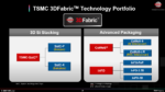
The TSMC 3DFabric is a comprehensive family of 3D Silicon Stacking and Advanced Packaging Technologies:
- TSMC 3DFabric consists of a variety of advanced 3D Silicon Stacking and advanced packaging technologies to support a wide range of next-generation products:
- On the 3D Si stacking portion, TSMC is adding a micro bump-based SoIC-P in the TSMC-SoIC®family to support more cost-sensitive applications.
- The 2.5D CoWoS®platform enables the integration of advanced logic and high bandwidth memory for HPC applications, such as AI, machine learning, and data centers. InFO PoP and InFO-3D support mobile applications and InFO-2.5D supports HPC chiplet integration.
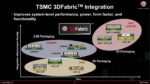
- SoIC stacked chips can be integrated in InFO or CoWoS packages for ultimate system integration.
- CoWoS Family
- Aimed primarily for HPC applications that need to integrate advanced logic and HBM.
- TSMC has supported more than 140CoWoS products from more than 25
- All CoWoS solutions are growing in interposer size so they can integrate more advanced silicon chips and HBM stacks to meet higher performance requirements.
- TSMC is developing a CoWoS solution with up to 6Xreticle-size (~5,000mm2) RDL interposer, capable of accommodating 12 stacks of HBM memory.
- InFO Technology
- For mobile applications, InFO PoP has been in volume production for high-end mobile since 2016 and can house larger and thicker SoC chips in smaller package form factor.
- For HPC applications, the substrateless InFO_M supports up to 500 square mm chiplet integration for form factor-sensitive applications.
- 3D Silicon stacking technologies
- SoIC-P is based on 18-25μm pitch μbump stacking and is targeted for more cost-sensitive applications, like mobile, IoT, client, etc.
- SoIC-X is based on bumpless stacking and is aimed primarily at HPC applications. Its chip-on-wafer stacking schemes feature 4.5 to 9μm bond pitch and has been in volume production on TSMC’s N7 technology for HPC applications.
- SoIC stacked chips can be further integrated into CoWoS, InFo, or conventional flip chip packaging for customers’ final products.
“Chiplet stacking is a key technology for improving chip performance and cost-effectiveness. In response to the strong market demand for 3D IC, TSMC has completed early deployment of advanced packaging and silicon stacking technology production capacity, and offers technology leadership through the 3DFabricTM platform,” said Dr. Jun He Vice President, Operations / Advanced Packaging Technology & Service, and Quality & Reliability. “With the production capacity that meets our customers’ needs, we will unleash innovation together and become an important partner that customers trust in the long term.”
TSMC’s customer centric culture will be a big part of the chiplet packaging revolution. By working with hundreds of customers you can bet TSMC will have the most comprehensive IC packaging solutions available for fabless and systems companies around the world, absolutely.
TSMC Press Release:
TSMC Announces the Opening of Advanced Backend Fab 6, Marking a Milestone in the Expansion of 3DFabric™ System Integration Technology
Also Read:
TSMC Clarified CAPEX and Revenue for 2023!
TSMC 2023 North America Technology Symposium Overview Part 1
TSMC 2023 North America Technology Symposium Overview Part 2
TSMC 2023 North America Technology Symposium Overview Part 3
TSMC 2023 North America Technology Symposium Overview Part 4
TSMC 2023 North America Technology Symposium Overview Part 5