The biggest surprise embedded in the Intel 22nm SoC disclosure is that they still do NOT use Double Patterning which is a big fat hairy deal if you are serious about the SoC foundry business. The other NOT so surprising thing I noticed in reviewing the blogosphere response is that the industry term FinFET was dominant while the Intel invented term Tri-Gate was rarely used.
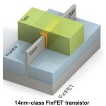
The transistor pitch – essentially the distance between two transistors – in the 22nm tri-gate technology is 80nm, which is the smallest pitch that can be produced using single-pattern lithography, Bohr says. “The next generation, 14,” he said, “we’re going to have to convert to Double Patterning to get tighter pitches.”
Mark Bohr is the infamous Intel Senior Fellow who mistakenly predicted the doom of the fabless semiconductor ecosystem. Mark is a funny guy. I remember him putting up an incomplete 22nm defect density trend slide at this year’s Intel Developers Forum and saying “Was it a mistake that I left the numbers out? Yes! Oh my goodness, how could I have done that? But, gee, time is up, so … ”
TSMC on the other hand presents their process defect density numbers every year at the TSMC Tech Symposium. Transparency equals trust in the foundry business, believe it.Back to Double Patterning, I will defer to the experts at Mentor for a complete description. Please see the Double Patterning Exposed articles for technical detail. No registration is required, just click on over.
So the question is: Why does TSMC use the extra lithography steps of Double Patterning for 20nm and Intel does not for 22nm? The answer is Restrictive Design Rules which essentially eliminates any variability in orientation of shapes on critical layers. Intel is very comfortable with incredibly restrictive design rules since they are a microprocessor manufacturer and not a pure-play foundry. Intel can micromanage every aspect of design and manufacturing down to the electron. TSMC on the other hand needs to accommodate different design requirements and intellectual property from 615 customers.In addition to more flexible metal routing, Double Patterning also enables a tighter metal pitch which will put TSMC 16nm head-to-head with Intel 14nm even though, as I explained in 16nm FinFET Versus 20nm Planar, 16nm FF leverages 20nm process technology.
It will be interesting to see how Intel tackles the Double Patterning challenge without the support of the mighty fabless semiconductor ecosystem.Which brings me to another trending topic: Is 20nm Planar a full node, half node, or everybody gonna skip node?
I can tell you as a matter of fact that the top semiconductor companies around the world will NOT skip 20nm. 20nm tape-outs are happening now with production silicon late next year. 20nm will require more processing time from GDS to wafer but it will NOT be cost prohibitive for high volume customers. You are probably familiar with the 80/20 rule where 80% of something or other is controlled by 20% of the people, in the semiconductor industry we call it the 90/10 rule where 90% of the of the silicon shipped is by 10% of the companies and you can bet that they will tape out at 20nm. Designing at 20nm planar will also make the transition to 16nm FinFET easier and I can tell you that EVERYONE will be taping out at 16nm FinFET. That’s my story and I’m sticking to it.
My favorite Mark Bhor quote: “We don’t intend to be in the general-purpose foundry business, I don’t think the volumes ever will be huge for Intel”. Exactly! So what is Intel going to do with all that empty fab space?