Where will Apple Manufacture the next iPhone Brain?

Where will Apple Manufacture the next iPhone Brain?
by Daniel Nenni on 07-17-2013 at 5:00 pm

There still seems to be a lot of confusion here so let me set the record straight. In regards to the Apple Ax SoC, the Apple iPhone 5s will have Samsung 28nm Silicon. Samsung 28nm is still ramping but Samsung can make enough wafers and eat the yield issues no problem. The Apple iPhone 6 in 2014 will have TSMC 20nm as I reported previously. TSMC 20nm is ahead of schedule so no problem there. Contrary to what was reported (TSMC reaches deal with Apple to supply 20nm, 16nm and 10nm chips, sources claim), the iPhone 6s in 2015 will have Samsung 14nm Silicon. Samsung is a bit ahead of the pack on FinFETs and from what I was told they made a wafer price offer that Apple could not refuse. As I mentioned before, there will be a glut of 16/14nm wafers so pricing will be VERY attractive for the fabless semiconductor industry. Best of luck to all who oppose us fabless people, you will need it.

This is all fact. Moving forward is opinion but I have a much better record on being right than my counterparts in regards to the fabless semiconductor ecosystem so keep on reading:

It is being reported that Apple will invest in a fab: Exclusive: Apple has a fab, will make their own chips. This is a complete FABrication. The SemiAccurate website has not even been semi accurate in regards to the foundry business. They have also changed business models so now you have to pay $1,000 to be a member of a rumor website? Good luck with that. I met the site’s owner Charlie Demerjian at CES in Las Vegas two years ago. Lets just say that he may talk tough behind a keyboard but in person, not so much. Charlie was wrong about Apple manufacturing at Intel, he was wrong about TSMC 40nm and TSMC 28nm, and he is wrong here. No way is Apple going to buy into a fab, especially UMC. UMC is a second source foundry which means they are a year or two behind TSMC. The whole point to the fabless ecosystem is competition, the ability to choose wafer providers based on different business variables. No way can Apple/UMC compete with Intel, TSMC, and Samsung on technology and wafer costs. 450mm wafers are coming and Apple will try and compete with a 300mm fab investment?


An article from C/NET has Apple tying up with GLOBALFOUDNRIES:

Apple talking to Globalfoundries about U.S.-based chipmaking, says report. If Apple owned capacity at a fab, it would give the company the kind of control over both design and chip manufacturing that Intel has.

This is not true. Apple started with Samsung as an ASIC customer and has worked for 5+ years to get out from under Samsung and be able to independently participate in the fabless semiconductor ecosystem. Apple does all of their own design work now. Apple even develops foundation semiconductor IP. Apple has successfully moved production from Samsung 28nm to TSMC 20nm. Samsung 28nm is gate-first HKMG technology and TSMC 20nm is gate-last HKMG with double patterning so that change was no small feat. Do a search on LinkedIn for Apple employees under the semiconductor category. You will see hundreds of experienced semiconductor professionals at Apple. You will also see a group of former ATI employees who have recently joined Apple for custom GPU development. Yes, Apple is designing their own GPU.

Bottom line: No way will Apple tie up to one foundry and give up the competitive advantages of the fabless semiconductor ecosystem. Not going to happen. There is a reason why we are all fabless now and I do not see Intel or anyone else turning back time to the Jurassic semiconductor period where “real men have fabs” weighing down their balance sheets, just my opinion of course.


The Future of Mobile Semiconductor Devices

The Future of Mobile Semiconductor Devices
by Daniel Nenni on 06-30-2013 at 5:00 pm


During my trip to Taiwan I hopped on over to Hong Kong for a speaking engagement. One of the things I do as an “Internationally Recognized Industry Expert” is help the financial world understand the semiconductor landscape as it pertains to SoCs and mobile devices. Usually I do this over the phone or in writing but I prefer to do it in person whenever possible. Nothing compares to the human connection with eye contact and a firm handshake. The Q&A part is my favorite since I get to ask questions too.

I generally start with a brief history of the fabless semiconductor industry then talk about specific technologies in use today, the major players in the market, and where I see them going forward. The examples I use are from my work with the top fabless semiconductor companies, the foundries, and the design enablement ecosystem (EDA and IP). That takes about 45 minutes I then open it up for questions. The big question is what will happen to the semiconductor landscape in the coming years? For me, the “coming years” means the coming semiconductor process nodes, 20nm, 16nm, and 10nm.

Mobile devices will continue to drive the semiconductor industry into the foreseeable future, no surprise there. 28nm was a bit of a shocker when TSMC was the only semiconductor manufacturer to yield which resulted in an unheard of > 90% market share. This caused shortages and the highest wafer margins we will probably ever see. Critics blame TSMC for the 28nm shortage but let’s face facts, the other foundries did not yield as forecasted and TSMC did not build capacity for > 90% market share.

20nm will be a half node since 16/14nm (20nm with FinFET transistors) is only one year behind. FinFETs offer significant power savings so the mobile people will be FinFETing as fast as they can. The high performance companies will probably skip 16nm to focus on 10nm which will arrive two years later. If you are betting against these dates be sure and hedge those bets because you will lose. The fabless semiconductor ecosystem is a force of nature, there is no stopping it now.

As it stands today there will be (6) foundries manufacturing FinFETS: Intel, Samsung, TSMC, GLOBALFOUNDRIES, UMC, and SMIC. If they all yield, which is a big IF, there will be a serious glut of FinFET wafers on the market. Even if only Intel, Samsung, and TSMC yield, which is NOT a big if, there will be a wafer glut. A softening global economy will put even more pressure on wafer pricing.

So what happens next? A price war of course, a price war of epic proportions, a game changing price war that will benefit the mobile market and the fabless semiconductor ecosystem but will change the foundry landscape for sure. Who will win the price war? Samsung of course. Samsung is no stranger to wafer dumping, which is how they dominated the DRAM market. Samsung is dominating the mobile market in the same manner, by flooding it with product. Samsung’s goal is to be the #1 semiconductor company and I honestly believe they will be.

Let’s not forget Intel was once a dominant player in the memory market. Unfortunately increased manufacturing competition from Asia dramatically reduced margins. As the story goes, Intel’s Andy Grove and Gordon Moore are talking about a board meeting the next day. “What do you think would happen if they fire us?” Grove said. “They’ll hire someone who’ll get us out of memories” Moore replied. “So why don’t we walk out of that door, come back in and do that ourselves.” And they did.

I cannot think of a more exciting time in the history of semiconductors. TSMC creating the fabless semiconductor ecosystem 25 years ago was exciting but FinFETs and the plethora of low cost mobile devices that are coming ranks right up there!

lang: en_US


What is inside the iPhone5s? Samsung or TSMC?

What is inside the iPhone5s? Samsung or TSMC?
by Daniel Nenni on 06-26-2013 at 6:00 pm

As a semiconductor professional and an Apple customer I’m very interested to see what is inside the iPhone5s. Rumors are spreading, photos are leaking, creating a nice build up to the next release of the mobile device that changed the world.

Honestly, last year I was a bit disappointed with the iPhone5. Inside is the A6 SoC which uses the Samsung 32nm process technology, even though Samsung announced a fully qualified 28nm process in June of 2011 (Can Samsung Deliver?). As a result, rumors swirled that Apple would switch to TSMC 28nm, rumors which I found to be false (TSMC Apple Rumors Debunked). So no, sad to say the iPhone5s will not have a TSMC 28nm SoC. My guess is that it will be Samsung 28nm which is said to be in production now.

Unless the iPhone5s has some cool new features like finger print scan and NFC for quick coffee house purchases, I will probably wait for the TSMC 20nm powered iPhone6 next year.

The other rumor that came out of Taiwan this week from DigiTimes is that Apple signed an agreement with TSMC for 20nm, 16nm, and 10nm. I’m in Taiwan now and can tell you that NOBODY here takes DigiTimes seriously. Same thing goes for Seeking Alpha, DeepChip, SemiAccurate, and other click hungry rumor websites. TSMC has beefed up security in the recent months so I seriously doubt that type of information leaked out here. Apple is also VERY secretive so I think it is just one of those tabloid journalism attempts to catch your eye.

From my discussions at the 50th Design Automation Conference, the top fabless companies are still looking closely at the different FinFET processes, waiting for the final PDKs (Process Design Kits) to be delivered later this year. Given the capacity issues at 28nm (since only TSMC yielded), I fully expect the fabless industry to keep second and even third source FinFET options open. As for who wins the node with the most first source contracts? It will be a tight race between TSMC, GLOBALFOUNDRIES, and Samsung with wafer price being the critical factor. My bet of course is on TSMC since they have the required capacity for mobile and trust is always part of the wafer purchase equation.

From what I know today, all three foundries will be ready for FinFET tape-outs in Q4 of this year. Here is my personal score card for the top fabless semiconductor companies on where they will manufacture FinFET Devices next year:

[LIST=1]

  • Apple @ TSMC and Samsung
  • Qualcomm @ TSMC, GLOBALFOUNDRIES, Samsung
  • Nvidia @ TSMC and Samsung
  • Xilinx @ TSMC
  • Altera @ Intel
  • Broadcom @ TSMC and GLOBALFOUNDRIES
  • NXP @ TSMC
  • Freescale @ TSMC
  • Mediatek @ TSMC and GLOBALFOUNDRIES
  • Marvell @ Samsung

    This of course is subject to change when the 1.0 production version of the PDKs (Process Design Kits) are released. TSMC could sweep the entire node like they did at 28nm and 20nm. But for someone to say that any of these companies has signed a foundry deal for 10nm is just silly. 10nm negotiations have just started and will absolutely hinge on who delivers 16nm as promised and at what price. All of this is just my opinion of course but let common sense prevail!

    lang: en_US


  • TSMC and Xilinx on the FinFAST Track!

    TSMC and Xilinx on the FinFAST Track!
    by Daniel Nenni on 06-23-2013 at 2:00 am

    The power of the fabless semiconductor ecosystem never ceases to amaze me. On one hand you have the Intel backed press crowing about Intel stealing Altera from TSMC. On the other hand you have Xilinx and TSMC crowing about a new ‘one-team’ approach. If you are interested in the real story you’ve come to the right place.

    “Altera’s FPGAs using Intel 14 nm technology will enable customers to design with the most advanced, highest-performing FPGAs in the industry,” said John Daane, president, CEO and chairman of Altera. “In addition, Altera gains a tremendous competitive advantage at the high end in that we are the only major FPGA company with access to this technology.”

    “I am extremely confident that our ‘FinFast’ collaboration with TSMC on 16-nanometer will bring the same leadership results that we enjoyed at previous advanced technologies,” said Moshe Gavrielov, President and CEO of Xilinx. “We are committed to TSMC as the clear foundry leader in every dimension, from process technology to design enablement, service, support, quality, and delivery.”

    The one disadvantage of the fabless semiconductor ecosystem and crowd sourcing in general is that you are working with companies that also work with your competitors. That is certainly the case with TSMC since just about every fabless semiconductor company manufactures at TSMC and TSMC is bound by honor (The Trusted Technology and Capacity Provider) to provide a level playing field for all customers. The only thing worse would be if the company that manufactures your product competes directly with you, just ask Apple!

    “We look forward to collaborating with Altera on manufacturing leading-edge FPGAs, leveraging Intel’s leadership in process technology,” said Brian Krzanich, chief operating officer, Intel. “Next-generation products from Altera require the highest performance and most power-efficient technology available, and Intel is well positioned to provide the most advanced offerings.”

    “We are committed to working with Xilinx to bring the industry’s highest performance and highest integration programmable devices quickly to market,” said Morris Chang, TSMC Chairman and CEO. “Together we will deliver world-class products on TSMC’s 20SoC technology in 2013 and on 16FinFET technology in 2014.”

    This was certainly the case for Altera and Xilinx at TSMC. The flow of information and collaboration was definitely guarded knowing full well that any process improvement would benefit both companies. Altera moving to Intel changed that of course, a change for the better in regards to the greater good of the fabless semiconductor ecosystem. Putting the number one foundry (TSMC) in close collaboration with the number one provider of programmable technologies and devices (Xilinx) could be a serious game changer, absolutely. Look for a Xilinx flavored version of the 16nm process for higher performance applications like FPGAs, CPUs, and GPUs. Just my opinion of course.

    Let’s look at the FUD side of this:

    • Intel as a foundry is an unknown
    • How fast will Altera be able to build a competitive Intel based ecosystem?
    • Intel as an FPGA manufacturer is an unknown
    • Will Intel eat crow and sign an ARM Manufacturing deal? (ARM cores are big in the FPGA world)
    • Or will Intel force Atom on Altera?
    • What happens to the other Intel FPGA partners Tabula and Achronix?

    I’m not questioning Altera’s decision to partner with Intel. It was definitely the right thing to do given Xilinx seriously challenged them at 28nm and will again at 20nm. Competition fuels our industry and Intel/Altera are a competitive threat so it is for the greater good.

    I do however question the Intel biased spin on the situation and the constant bashing of the fabless semiconductor ecosystem. My opinion, Intel will rue the day they openly attacked QCOM, ARM, TSMC, and the rest of the fabless crowd, believe it. Hey Mr. Intel, this is not the microprocessor world you have controlled since the beginning of time. You are not in Kansas anymore Dorothy.

    lang: en_US


    Taiwan Semiconductor Tries To Pull A FinFAST One!

    Taiwan Semiconductor Tries To Pull A FinFAST One!
    by Daniel Nenni on 06-16-2013 at 7:00 pm


    This completely misleading title is from a Seeking Alpha (SA) article, a stock investment version of the National Enquirer. As I mentioned inA Call to ARMs, fame and fortune seeking SA Authors make a penny per click so sensationalism sells. The article is not worth your time so I will save you the click and skip to the misguided conclusion:

    TSMC is a great company that is a leader in the foundry space, but they are trying too hard to appease investors/customers with some of these claims regarding FinFETs. On the January call (before Intel took Altera and likely Cisco (CSCO) from TSMC), the claim was “minimal volumes of 16nm in 2015”. Now, TSMC is trying to pull a FinFAST one on investors and customers by claiming that 16nm will be in production during 2014, totally bypassing the yet-to-ramp 20nm node.I’m not buying these claims, and neither should you.

    First, you should know that Cisco is an IBM ASIC customer not a TSMC customer. ASIC customers do the front half of the design while letting the ASIC vendor (IBM) complete the chip. TSMC does not do ASICs, to be a TSMC customer Cisco will have to go through a services provider such as Global Unichip or LSI Logic. IBM is getting out of the ASIC business so Cisco switching to Intel is a smart move. Today Intel does not have the ecosystem required to allow fabless semiconductor companies to use their fabs without training wheels so the ASIC model works for Intel. Seeking Alpha is promoting F.U.D. (fear, uncertainty, and doubt) here.

    Second, here is a FinFET update: As a SemiWiki reader you should know that I have spent a lot of time on FinFETs since hearing about them at ISSCC in 2011:

    “New transistor designs are part of the answer,” said Dr. Jack Sun. “Options include a design called FinFET, which uses multiple gates on each transistor. Researchers have made great progress with FinFET, and TSMC hopes it can be used for the next generation of CMOS — the industry’s standard silicon manufacturing process.”

    Immediately following, I asked friends and co-workers why TSMC did not already have FinFETs on the road map. The answer from the top fabless companies was that changing transistor architecture is a huge risk and the reward of FinFETs was not clear to them at that time. This was back before 28nm when the top mobile designers chose 28nm polyscion over HKMG for the same reason, lower risk. Leading edge semiconductor designers are by nature risk adverse.

    Let us not forget where FinFETs came from: Dr Chenming Hu, the father of FinFETs, and this year’sKaufman Award winner. Chenming’s ground breaking work on FinFETs and the BSIM modeling standard were the highlights of his technical achievements. Chenming is a former TSMC CTO and today is a TSMC Distinguished Professor at UC Berkeley. TSMC knows FinFETs, believe it.

    Disclaimer: The following FinFET information comes from sessions and private discussions at the 50[SUP]th[/SUP] Design Automation Conference this month, not from Googling around and making foolish assumptions to support my stock positions.

    Today the top fabless semiconductor companies have taped-out 20nm designs which will go into production in 2014. 20nm is now ramping, silicon IS correlating (working), I see no barriers to full production in 2014. TSMC estimated that 20nm revenue would start in Q2 2014 but my bet is they are being conservative by one quarter to appease Wall Street. Either way your iPhone6 will have TSMC 20nm Silicon next year, believe it.

    FinFETs are also ahead of schedule. Remember, the first version of FinFETs will use the 20nm process so delivering them in one year versus the standard two year new process technology launch is not unexpected or unrealistic to the experienced semiconductor professional. Consider 16nm to be a half node in regards to development time and delivery.

    Today the 16/14nm version .5 PDKs (process design kits) are in use by the leading fabless semiconductor companies. The 1.0 PDKs will be released in October with tape-outs shortly thereafter. If the PDK change between version .5 and version 1.0 is minimal, tape-outs will happen in Q4 of 2013 with production/revenue STARTING one year later (just in time for the iPhone7). If the 1.0 PDK has significant changes tape-outs may be delayed to Q1 2014. Keep reading SemiWiki and you will be one of the first to know.

    The other interesting FinFET news is that the foundries will most likely offer two versions of the 16/14nm process: a low power version and a version with more performance. From what I understand the transistor thresholds and pitches will be adjusted for performance. Not a big change but hopefully it will get an extra 10% or more speed-up for those who need it.

    So again Seeking Alpha is publishing FinFALSE information to satisfy personal agendas of the Authors. Just my opinion of course.

    lang: en_US


    Meeting with Sidense at TSMC Technology Symposium

    Meeting with Sidense at TSMC Technology Symposium
    by Eric Esteve on 06-10-2013 at 11:34 am

    If you have attended DAC in Austin (June 2-5), you probably have missed the first TSMC Technology Symposium. It was held on June 6 in Shanghai. Considering my own experience of a 29 hours trip to come back home (in France), I doubt that it was any possible to leave Austin on June 5 to attend TSMC Technology Symposium in Shanghai on June 6, even flying a 2X supersonic airplane (the trap is the 13 hours time difference between both cities – in the wrong direction, leaving only a couple of hours to make it!).
    But, if you want to meet with Sidense at TSMC Technology Symposium, you still can make it if you live close to:

    • Amsterdam, the Symposium will be on June 18
    • Herzliya (Israel), it will be on June 26
    • Yokohama (Tokyo) on June 28

    On a map, Yokohama looks far from Tokyo by car, but if you take the Shinkensen (Japanese High Speed train), you will be surprised how fast you arrive. The point is just to read Japanese characters in Tokyo station to find the right platform, or ask your way, that I did successfully!
    Just remember that Sidense is the OTP NVM IP vendor who has recently won an interesting case as I blogged here: The decision made by United States Court of Appeals for the Federal Circuit, “Affirming” the District Court for the Northern District of California’s summary judgment of non-infringement on Kilopass’ patent claims and its dismissal, with prejudice, of all remaining claims against Sidense, is certainly a good news for IP and EDA vendors playing a fair sales and marketing game in the field. Let’s make the assumption that you have not infringed anybody else rights, but developed innovative product (IP function or EDA tool), be clever enough in marketing the product and generate numerous design win, so your sales revenue start growing fast, leading your direct competitor to prefer using the legal field instead of fair market competition… We have seen many legal cases in the recent years in the EDA and IP ecosystem, and I am almost sure that some of these cases have been initiated to compensate for a marketing weakness.

    To go to TSMC Technology Symposium, just register here, and you could visit Sidense and discuss about OTP NVM IP, much more interesting topic than legal battle.

    Eric Esteve from IPNEST –

    lang: en_US


    The Morphing of Intel’s Monopoly

    The Morphing of Intel’s Monopoly
    by Ed McKernan on 05-09-2013 at 12:01 am

    It was a generation ago when Intel, less than three years old, created the three fundamental building blocks of the compute era: the DRAM, the EPROM and the Microprocessor, an incredible feat of innovation by any measure. Manufacturing yield, not power or performance determined success of failure and in the first two Continue reading “The Morphing of Intel’s Monopoly”


    IP Quality: Foundation of a Successful Ecosystem

    IP Quality: Foundation of a Successful Ecosystem
    by Eric Esteve on 05-08-2013 at 8:46 am

    Talking about Design IP (I mean successful Design IP) lead you to quickly pronounce the two magic key words: Quality and Ecosystem. Those who remember the IP emergence in the mid 90’s know very well why Quality has to be a prerequisite when dealing with Design IP, as they probably have paid the price of mediocre IP quality at that time. More recently, business analysts have realized that the foundation for a successful IP based business was linked to building a complete Ecosystem, just think about the 1000 ARM partners…

    As a matter of fact, some of these partners are heavyweight, like Taiwan based TSMC, that any IP vendor would like to count within it IP Ecosystem. That’s why TSMC has created, back in 2000, the TSMC9000 program as one of the pillar of Open Integration Platform (OIP) ecosystem. TSMC9000 clearly defined goal is to check for, assess and audit the quality of Design IP part of OIP ecosystem. TSMC9000 is not only based on cleaver communication, but on a very rigorous process! Don’t forget that any of this Design IP function will end up into a very concrete piece of Silicon, an Integrated Circuit, and that both TSMC (who process it into Wafer Fab) and the Fabless customer who plan to sell it, expect this IC to run first time right. As an IP vendor, you submit to TSMC (in fact to “IP Portfolio, Design Infrastructure Division”) the functional IP you have developed, from USB PHY to DDR Memory Controller, LVDS I/O to DSP and many more. TSMC9000 Quality Assurance system consists to run successively:

    • DRC/LVS (if you submit Hard IP)
    • Data Consistency check
    • ESD tolerance verification
    • Design margin verification (Shmoo plot)
    • Then generate Silicon reports (on Test chips) and store production history when it’s relevant.

    Your IP will hopefully be sold to customer, integrated into a design data base by this customer who will finally submit the final DB for Tape Out. At this stage, TSMC will use “IP Master” tool, running “Tape Out consistency checks” versus the previously generated data in IP9000 IP Quality.

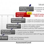
    You may wonder that TSMC9000 IP qualification process only applies to very complexes or very specific or “exotic” Design IP… In fact, if you take a look at the above picture, you realize that TSMC9000 apply to ALL the Libraries, Memories or IP, including Hard and Soft IP. How many IP would you guess? Are we talking about 500 Design IP, or 1000, maybe 2000? Just take a look at the statistics listed below…

    There are no less than 8917 active IP coming from the IP Alliance for a total of almost 10, 000 IP in TSMC 9000! Another figure is surprising: almost 200 Design IP are being reviewed every month by TSMC. This means that TSMC has built a specific team 100% dedicated to run IP9000 QA Process, a 30 people team in charge of IP Port-Folio validation (and selection). As an IP vendor, you probably better understand why TSMC has to be highly selective when accepting new IP… Are you still in IP vendor shoes? Just look at the failed TSMC 9000 IP count: 1,452!!

    Even if a dummy density violation or some Silicon corner out of specification can be accounted for a failure, out of these 1,452 IP, as high as 373 can generate potential fatal failure. Fatal simply means that a Tape Out including such IP would have led to a redesign. Thus, if you go now into Fabless shoes, you will just thank your foundry supplier for being so selective!

    If you ever surfed on a foundry web site, you probably remember the “Bronze”, “Silver” and “Gold” denomination for Design IP. If you look at the above picture, these denominations look a little bit obsolete: before a Design Hard IP can be validated for volume production, it has to pass through no less than ten or more verification phases, before the Design IP can reach a high enough confidence level. If we consider advanced nodes, the Hard IP has to pass through 13 various checking phases, from DRC, LVS, ERC and Antenna checks up to Split Lot Silicon Assessment, testing results audits by TSMC test lab to finally go to production. In fact, Quality assessment is a never ending process, when the ASIC or ASSP is in volume production, the IC yield is continuously traced… probably up to the product End Of Life!
    I didn’t know that Quality could be a fascinating topic (to be honest, I thought it was not), but we are working in such demanding industry that even Quality becomes part of the dream: I have today in my pocket a gaming station from the 2000’s, a phone from the 90’s, a color TV from the 80’s and a Supercomputer from the 70’s, all of these almost in a single chip!

    Eric Esteve

    lang: en_US


    How To Design a TSMC 20nm Chip with Cadence Tools

    How To Design a TSMC 20nm Chip with Cadence Tools
    by Paul McLellan on 05-07-2013 at 8:10 pm

    Every process node these days has a new “gotcha” that designers need to be aware of. In some ways this has always been the case but the changes used to be gradual. But now each process node has something discontinuously different. At 20nm the big change is double patterning. At 14/16nm it is FinFET.

    Rahul Deokar and John Stabenow of Cadence and Jason Chen from TSMC will present, “20nm Design Methodology: A Completely Validated Solution for Designing to the TSMC 20nm Process Using Cadence Encounter, Virtuoso, and Signoff tools.” Well, I think my title gets to the point a bit quicker!


    Double patterning has been forced on us by limitations in lithography. We still use 193nm light even though we are now drawing features that are 20nm (actually there isn’t really anything on a 20nm chip that measures 20nm). If we try and draw all the polygons on the lower layers of the process, the features are too close to print correctly. So instead we have to separate them onto two separate masks, so the polygons in effect alternate. Not all layout can be split in this way, which is usually called coloring since it is basically a graph-coloring algorithm, so routers and designers need to be careful not to create uncolorable layout.

    Sometimes, even (say for analog), the designer wants to color the polygons manually. Why would they do that? At this process node, the two masks are not self-aligning. They are aligned by the vestigials on the wafer that the stepper detects, just like any other mask (actually reticle) but the two polygon layers have some slop in their alignment. This means that there is much tighter control of parasitics between polygons on the same mask (which are automatically self-aligning) and different masks (which are not).

    There are self-aligned double patterning techniques. They use a sacrificial spacer (where both sides of the spacer eventually get whatever is being created on that layer) but they are more expensive. If you want to get a few chapters ahead, we will need to use these approaches to build transistors at the 10nm node (and maybe the lower levels of interconnect) but at 20nm we are not. I’m not sure about 16nm.

    The layout rules for 20nm are very much more restrictive, even without worrying about double patterning. There is a lot less flexibility about what can go where, and weird features like dummy gates that we started to see at 28nm (where an extra poly is required on the end of a gate that is not electrically significant, to ensue that the gate prints and behaves correctly). We also have layout dependent effects (LDE) where the transistor circuit level performance depends on how close the transistor is to other features on the die, especially well boundaries. And even design rules that depend on electrical details. There is also local interconnect that appears between the transistors and the lowest level of true metal, with all its own rules.


    A little more detail on what you will learn:

    • How in-design double patterning technology (DPT) and design rule checking (DRC) can improve your productivity
    • How both colored and colorless methodologies are supported, and data is efficiently managed in front-to-back design flows
    • How local interconnect layers, SAMEMASK rules, and automated odd-cycle loop prevention are supported
    • How mask-shift modeling with multi-value SPEF is supported for extraction, power, and timing signoff.

    The webinar is being given twice on May 23rd at 9am Pacific (early evening in Europe) and at 6.30pm Pacific (morning in Asia). Details here. Registration here.