The design community is always hungry for high-performance, low-power, and low-cost devices. There is emergence of FinFET and FDSOI technologies at ultra-low process nodes to provide high-performance and low-power requirements at lower die-size. However, these advanced process nodes are prone to new sources of variation. Moreover, cutting-edge designs with best PPA (Power, Performance, and Area) leave very less design margins.
In such a situation with high variation and low design margin, the designers have to struggle doing more variation analysis, thus impacting design schedule. To achieve a successful design closure in time, it’s important that the variation analysis tool must be robust to provide high performance, accuracy, and coverage.
In 2015, at 52[SUP]nd[/SUP] DAC, Cypress, Applied Micro Circuits, and Microsemi had presented their successful stories about dealing with variations in their designs. They used Solido’s Variation Designer which is scalable over large number of process variables and prioritizes simulations for most-likely-to-fail cases. I had blogged about this at that time, the link is provided below; the blog also contains the links to their video presentations.
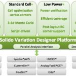
Over the year, the Variation Designer is further improved in verification speed, accuracy, and coverage for leading-edge designs with high-performance, low-power, and low-voltage. The Variation Designer platform has a very efficient variation debugging environment. This is the next generation ‘Variation Designer 4’ from Solido.
Solido will be coming up with their new developments in this year’s 53[SUP]rd[/SUP] DAC as well, but before that I wanted to highlight how TSMCand Solido are collaborating to realize variation-aware designs at advanced process nodes.
TSMC and Solido are jointly offering the following free webinar –
TSMC and Solido Collaborate for Variation-Aware Design of Memory and Standard Cell at Advanced Process Nodes
Abstract:
Variation effects have an increasing impact on advanced process nodes, and at each, new sources of variation must be considered. Furthermore, increased competition is forcing tighter design margins to make high-performance, low-power, low-cost products. Designers must now do more variation analysis than ever to achieve these tighter margins, using advanced variation-aware technology for speed, accuracy and coverage to deliver competitive chips on schedule. This webinar will discuss on how TSMC and Solido collaborate to offer variation-aware design techniques for memory and standard cell with TSMC advanced processes using Solido’s new Variation Designer 4.
Speakers– Jacob Ou, Technical Marketing Manager at TSMC (on left) andKristopher Breen,VP Customer Applications at Solido
Date: June 1, 2016
Time: 10am Pacific
Duration: 55 minutes
Click here to register!
Also read: Moving with Purpose for Certainty