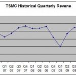
What Do You Mean by Mandatory?

What Do You Mean by Mandatory?
by glforte on 10-14-2010 at 6:00 pm

When TSMC and Mentor Graphics held a joint seminar for mutual customers to go over new DFM requirements at 45/40 nm, two customers basically asked the same question, “What do you mean by mandatory?” Of course, TSMC wasn’t going to stand over them and say, “Mandatory means mandatory, what part of mandatory don’t you understand?” :=) TSMC admitted that they hadn’t yet changed the tape-out checklist to forcibly include the DFM checks (CMP and LPC). This is what begs the question, what do you mean by mandatory?
Continue reading “What Do You Mean by Mandatory?”


What Do You Mean by Mandatory?

What Do You Mean by Mandatory?
by glforte on 10-14-2010 at 6:00 pm

When TSMC and Mentor Graphics held a joint seminar for mutual customers to go over new DFM requirements at 45/40 nm, two customers basically asked the same question, “What do you mean by mandatory?” Of course, TSMC wasn’t going to stand over them and say, “Mandatory means mandatory, what part of mandatory don’t you understand?” :=) TSMC admitted that they hadn’t yet changed the tape-out checklist to forcibly include the DFM checks (CMP and LPC). This is what begs the question, what do you mean by mandatory?
Continue reading “What Do You Mean by Mandatory?”


So, Why Not Just Write Better Rules?

So, Why Not Just Write Better Rules?
by glforte on 10-14-2010 at 4:00 pm

In my submission about TSMC making some DFM analysis steps mandatory at 45nm (see “TSMC’s DFM Announcement”), I ended with a question about why the foundries can’t just write better design rules (and rule decks) to make sure all designs yield well. Here’s my take on this complicated question.
Continue reading “So, Why Not Just Write Better Rules?”


TSMC’s DFM Announcement

TSMC’s DFM Announcement
by glforte on 10-14-2010 at 4:00 pm

If you are a TSMC customer, no doubt you have heard TSMC is requiring lithography and planarity analysis for all 45nm designs. Their website says customers can either run it themselves, or contract TSMC services to do it. The most cost-effective way would be for the customers to run it themselves, but some might not have the resources to do that. Of course, by the time you pay TSMC to do it 3 or 4 times, you could have bought some tools and run it yourself. That’s good for Mentor and other EDA vendors, right? Probably, but there has to be more to it than that.
Continue reading “TSMC’s DFM Announcement”


So, Why Not Just Write Better Rules?

So, Why Not Just Write Better Rules?
by glforte on 10-14-2010 at 4:00 pm

In my submission about TSMC making some DFM analysis steps mandatory at 45nm (see “TSMC’s DFM Announcement”), I ended with a question about why the foundries can’t just write better design rules (and rule decks) to make sure all designs yield well. Here’s my take on this complicated question.
Continue reading “So, Why Not Just Write Better Rules?”


TSMC’s DFM Announcement

TSMC’s DFM Announcement
by glforte on 10-14-2010 at 4:00 pm

If you are a TSMC customer, no doubt you have heard TSMC is requiring lithography and planarity analysis for all 45nm designs. Their website says customers can either run it themselves, or contract TSMC services to do it. The most cost-effective way would be for the customers to run it themselves, but some might not have the resources to do that. Of course, by the time you pay TSMC to do it 3 or 4 times, you could have bought some tools and run it yourself. That’s good for Mentor and other EDA vendors, right? Probably, but there has to be more to it than that.
Continue reading “TSMC’s DFM Announcement”


TSMC OIP Conference 2010 Critique!

TSMC OIP Conference 2010 Critique!
by Daniel Nenni on 10-10-2010 at 10:18 pm

Okay, this is more of a, “What I would do if I was TSMC” than a critique, but I needed a one word descriptor for the title. This was the third TSMC OIP Conference and I would guess about 250 people attended. This was the first time I have seen TSMC in “reactive” mode versus “proactive” leadership mode, so I was a bit disappointed. TSMC is THE industry leader and should NOT be looking in the rear view mirror at competitors that are barely visible.

The semiconductor landscape has dramatically changed during the contraction phase of the current business cycle. The strong got stronger by acquisition and aggressive business practices, and the rest of the fabless semiconductor companies either were: acquired, got smaller, or became IP companies. So TSMC, being a customer driven company, must also change strategies and the Open Innovation Platform IS the delivery system for that change.

The Pareto principle (also known as the 80-20 rule or the law of the vital few) states that, for many events, roughly 80% of the effects come from 20% of the causes. For semiconductors this is definitely the case. In fact, as a result of the recent economic chaos and consolidations I would guess that 90% of the silicon is shipped by 10% of the companies.

The foundry strategy for the top semiconductor companies is three-fold: Early Access, Capacity, and Wafer Pricing. TSMC is working hard on capacity and wafer pricing 24/7, believe it! There is no doubt in my mind that TSMC will continue to be the capacity and margin leader for 40nm, 28nm, and 20nm, which will keep the top foundry customers engaged. Early access however is a continuing challenge. For example, Design Rule Manuals (DRMS) are still in PDF format, 1,300+ pages long, and rapidly changing. Some of the rules are so complicated they are impossible to describe, and even harder to code and communicate, even within the foundry teams. This should be the focus of the TSMC OIP for the top semiconductor companies, a more automated and simplified information exchange, one that uses vendor neutral formats so customers cannot be held hostage by short sighted EDA vendors. The iPDK initiative is an excellent start but there is much more that can be accomplished.

For the other 90% of the semiconductor companies, the ones that cannot afford to develop custom design flows, PDK’s, and IP, the ones that cannot afford an in-house foundry team for early access, TSMC OIP is a critical enabler. Unfortunately, one of the messages of the conference was, “TSMC will not compete with partners”, which was a clear response to public relations pressure from the GlobalFoundries mantra, “We don’t compete with partners!”

Competition is what has made the semiconductor industry and semiconductors themselves what they are today! Competition is what drives innovation and keeps costs down. Not destructive competition, where the success of one depends on the failure of another, but constructive competition that promotes mutual survival and growth where everybody can win. The semiconductor design ecosystem is the poster child for destructive competition, which is why EDA ( SNPS, CDNS, MNTR, LAVA) valuations are a fraction of what they should be.

The TSMC Open Innovation Platform should be the cornerstone of the semiconductor design ecosystem. The ecosystem must NOT hold designers hostage with proprietary formats! The ecosystem MUSTinnovate to compete! The TSMC Open Innovation Platform MUST lead the way! TSMC is the #1 foundry and that will not change within my lifetime. TSMC must also be #1 in customer satisfaction and the design ecosystem ISwhere customer satisfaction begins.


TSMC GigaFab Tour!

TSMC GigaFab Tour!
by Daniel Nenni on 10-01-2010 at 9:44 am

During my most recent Taiwan trip I was not only afforded a meeting with Dr Mark Liu, Sr VP of TSMC, a guided tour of GigaFab #12 was also included. Even more impressive, I’m now considered “Elite” by Eva Airlines so I automatically get the good seats, better food, and VIP service. My wife, however, is not impressed with my Elite status so I still have to do chores around the house.

Mark Liu ramped up TSMC’s first 200mm fab in 1993 and has been building fabs for TSMC ever since. Mark’s favorite topic is the 300mm GigaFabs, Fab#12, Fab#14, and Fab #15 which TSMC just broke ground on last month. Clearly TSMC has learned a valuable lesson from the 40nm wafer shortage experience. Not having enough capacity is far more costly than having too much. After 40nm, customer priorities have certainly changed: Capacity is now the 1st concern with price a close 2[SUP]nd[/SUP], and last but not least design enablement. Please note that the perceived value of semiconductor design enablement is often overlooked but it is clearly the key enabler to TSMC’s expansive customer base.
After putting on the clean room space suit and being lightly air washed I entered a GigaFab for the first time and was literally speechless. If you know me personally, being speechless is not one of my strong suits so this was a new experience.

The insignias on the machines were logos and acronyms that I recognized but what struck me was the total automation of a GigaFab. Machines outnumbered man exponentially with 99% automation. Shuttles zoomed around on tracks above delivering thousands of 40nm wafers to the 300+ steps in the semiconductor manufacturing process. The few people I did see were at monitoring stations. Even more impressive than the billions of dollars of hardware in a GigaFab, is the millions of lines of software developed to run it: Automated Material Handling Systems (AMHS) for transporting, storing, and managing semiconductor wafer carriers and reticles plus Manufacturing Execution Systems (MES) software to manage overall production efficiency.

This year TSMC will spend a record $5.9B on capital expenditures. Approximately 75% will be used to expand TSMC’s 65/40/28nm technology capacity and 15% will be used for mainstream processes. The remainder will be used for equipment, R&D expenses, and new business such as solar and LED. TSMC’s newest Gigafab, Fab 15, will cost an estimated $9.4B. TSMC is also set to complete Phase 5 expansion at Fab 12, and Phase 4 expansion at Fab 14.

According to the most recent management report, TSMC has accelerated its capacity expansion plan for 2010. Total managed capacity was 2,749K 8-inch equivalent wafers in 2Q10, increased by 7% from 2,566K in 1Q10. Current capacity plan calls for an overall increase by 14% to 11,299 8- inch equivalent wafers, compared with 11,247 8-inch equivalent wafers planned in the last quarter.

Demand for TSMC’s advanced technology wafers in all major semiconductor market segments again increased quarter to quarter. Among the advanced technologies, 40nm not only increased an additional 2% of TSMC’s revenue share, the output of Gigafab wafers processed using 40nm technology increased by 30% sequentially.

The 40nm race is officially over, TSMC wins by a landslide in regards to capacity, price, and design enablement. The race for 28nm dominance however is still on between TSMC, Samsung, and GlobalFoundries. Samsung is in production at 32nm so moving to 28nm should just be a process shrink. For TSMC and GlobalFoundries, 28nm is a completely new node which will bring new technical challenges. Still, in my opinion, the foundry race to 28nm is too close to call today and it will certainly be an exciting finish!


Taiwan Semiconductor Manufacturing Corporation (NYSE: TSM)

Taiwan Semiconductor Manufacturing Corporation (NYSE: TSM)
by Daniel Nenni on 07-11-2010 at 10:09 pm

After working with TSMC the past 10+ years the single most compelling question I have is why the stock (NYSE: TSM) is not at record highs. TSMC invented and continues to dominate the foundry business which is clearly the future of modern semiconductor design and manufacture. So why is this not a $20+ stock?!?!?

TSMC reports 36%+ net margins.
TSMC delivers a 24%+ return on equity.
TSMC just announced a 3.8% dividend.
TSMC carries $6B+ total cash.
TSMC has more capacity than its top rivals combined and a third Gigafab under construction.
TSMC has almost a 7X Market Cap margin between its closest rival UMC.
So why is TSM flatlining after yet another record setting month of sales?!?!?

One of my favorite stock crowdsourcing groups agrees that TSM is undervalued. Based on the aggregate intelligence of 165k+ investors participating in Motley Fool CAPS, TSMC has a 5 out of 5 star rating. A Motley Fool CAPS rating indicates a stock’s potential to outperform the S&P 500 as determined by the community. On CAPS, 99% of the 437 All-Star members who have rated Taiwan Semiconductor Manufacturing Corporation believe the stock will outperform the S&P 500 moving forward.

Just how strong is TSMC in the global semiconductor foundry business? Well, with 45%+ market share, TSMC is about three times as big as its closest competitor, #2 foundry UMC, and more than six times as big as the #4 China based foundry SMIC. Even with the overly documented 40nm yield ramping problems, TSMC is still in charge of that node with an estimated 80% market share. Today, the race for 28nm is on with production silicon due out in Q1 2011. TSMC? GlobalFoundries? Samsung? It’s a 3 horse race, expect a photo finish, the winner is the King of the Node!

TSMC is expected to finish 2010 at $12.5B.
TSMC serves the largest and most diverse customer base.
TSMC will spend a record $4.8B on capital expansion this year.
TSMC will be trying to recruit 5,000 new employees this year.
TSMC is investing heavily in LED and Solar thin film PV technologies.
TSMC is the favorite to win the 28nm node foundry race next year.
TSMC has a 5 star Motley Fool CAPS rating.

Out of control consumer spending will continue to drive foundry revenues to record highs. Semiconductor industry mystics see foundry revenue growing 30-40% in 2010 and 8-10% annually over the next 4 years. Meanwhile, in 2010 shares of TSM and UMC are down 12% and 21%, respectively. So tell me again why TSM is yet another under performing tech stock?!?!


TSMC Unveils First Ever AMS Reference Flow!

TSMC Unveils First Ever AMS Reference Flow!
by Daniel Nenni on 06-08-2010 at 9:17 pm

As a quick follow-up to my blog TSMC Extends Open Innovation Platform, TSMC today announced the Analog/Mixed Signal Reference Flow 1.0., another key collaborative component of TSMC’s Open Innovation Platform™.

The TSMC AMS Design Flow 1.0’s design package is integrated seamlessly on top of the 28nm interoperable process design kit (iPDK) and OpenAccess database and includes:

  • Industry-first layout-dependent effect (LDE) aware design methodology
  • TSMC-specific LDE engine
  • Complete DFM-aware analog layout guideline and checker utility
  • Advanced analog base cell (ABC) design
  • Comprehensive design configuration management environment
  • A robust front-end design and simulation platform for the analysis of design sensitivity, yield, multi process corners, noise effect, IR drop and electromigration (EM) issues.
  • Constraint-driven analog placement and routing technology for fast layout prototyping, semi-automatic rule-driven layout assistance, and a demonstration of a PLL system design budgeting and loop filter layout synthesis capability.
  • A Physical verification flow that includes accurate 3D field solver based extraction with intelligent RC reduction, and full DRC/LVS sign-off and dummy pattern insertion and extraction.


“TSMC’s Open Innovation Platformdeliverscomprehensive and innovative designtechnology services that remove advanced technology adoption barriers. Ithelpslower design costs andimprovestime-to-market,” said Dr Fu-Chieh Hsu, Vice President of Design Technology Platform and Deputy Head of Research & Development. “TheOpen Innovation Platform willnow beginaddressing system-level design’s cost and complexity and enable packaging of entire electronic systems onto multi-chip packages.”

The TSMC AMS Reference Flow 1.0 is developed and fully validated in collaboration with multiple EDA partners including:

  • Apache Design Solutions
  • Berkeley Design Automation
  • Cadence
  • Ciranova
  • EdXact
  • Mentor Graphics
  • Magma Design Automation, Mentor
  • Pyxis Technology
  • Silicon Frontline
  • SpringSoft
  • Solido Design Automation
  • Synopsys

“The design ecosystem must move beyond its current bounds and embrace the systems- level challenges that are at the heart of every design consideration. The Open Innovation Platformbegan setting the standard for ecosystem collaboration two years ago. TSMCcontinues to answer the market’s calland will build that same collaborative spirit on a system-level basis,” explained S.T. Juang, senior director, Design Infrastructure Marketing at TSMC.