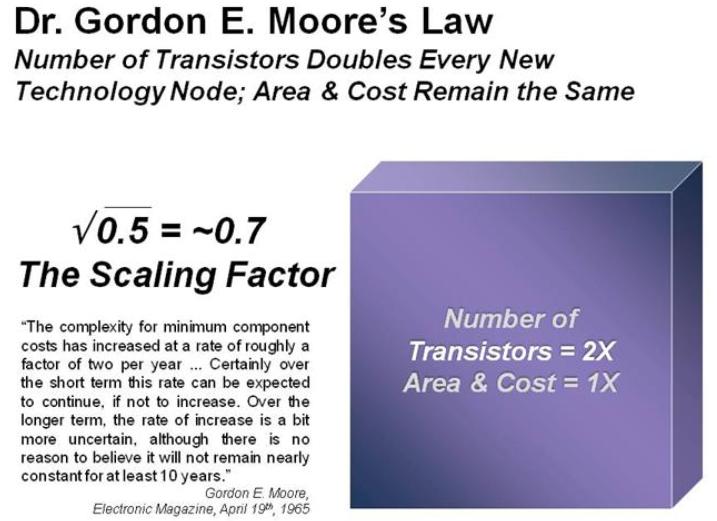

The semiconductor design and manufacturing challenges at 40nm and 28nm are a direct result ofMoore’s Law, the climbing transistor count and shrinking geometries. It’s a process AND design issue and the interaction is at the transistor level. Transistors may be shrinking, but atoms aren’t. So now it actually matters when even a few atoms are out of place. So process variations, whether they are statistical, proximity, or otherwise, have got to be thoughtfully accounted for, if we are to achieve low-power, high-performance, and high yield design goals.

"The primary problem today, as we take 40 nm into production, is variability,” he says. “There is only so much the process engineers can do to reduce process-based variations in critical quantities. We can characterize the variations, and, in fact, we have very good models today. But they are time-consuming models to use. So, most of our customers still don’t use statistical-design techniques. That means, unavoidably, that we must leave some performance on the table.”Dr. Jack Sun, TSMC Vice President of R&D

Transistor level design which lnclude Mixed Signal, Analog/RF, Embedded Memory, Standard Cell, and I/O, are the most susceptible to parametric yield issues caused by process variation.
Process variation may occur for many reasons during manufacturing, such as minor changes in humidity or tempature changes in the clean-room when wafers are transported, or due to non uniformities introduced during process steps resulting in variation in gate oxide, doping, and lithography; bottom line it changes the performance of the transistors.
The most commonly used technique for estimating the effects of process variation is to run SPICE simulations using digital process corners provided by the foundry as part of the spice models in the process design kit (PDK). This concept is universally familiar to transistor level designers, and digital corners are generally run for most analog designs as part of the design process.
Digital process corners are provided by the foundry and are typically determined by Idsat characterization data for N and P channel transistors. Plus and minus three sigma points maybe selected to represent Fast and Slow corners for these devices. These corners are provided to represent process variation that the designer must account for in their designs. This variation can cause significant changes in the duty cycle and slew rate of digital signals, and can sometimes result in catastrophic failure of the entire system.
However, digital corners have three important characteristics that limit their use as accurate indicators of variation bounds especially for analog designs:
- Digital corners account for global variation, are developed for a digital design context and are represented as “slow” and “fast” which is irrelevant in analog design.
- Digital corners do not include local variation effects which is critical in analog design.
- Digital corners are not design-specific which is necessary to determine the impact of variation on varying analog circuit and topology types.
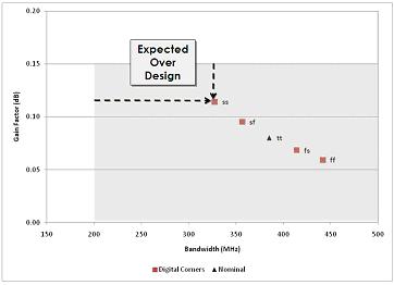
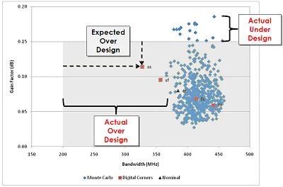
These characteristics limit the accuracy of the digital corners, and analog designers are left with considerable guesswork or heuristics as to the true effects of variation on their designs. The industry standard workaround for this limitation has been to include ample design margins (over-design) to compensate for the unknown effects of process variation. However, this comes at a cost of larger than necessary design area, as well as higher than necessary power consumption, which increases manufacturing costs and makes products less competitive. The other option is to guess at how much to tighten design margins, which can put design yield at risk (under-design). In some cases under and over-design can co-exist for different output parameters for a circuit as shown below. The figure shows simulation results for digital corners as well as Monte Carlo simulations which are representative of the actual variation distribution.
To estimate device mismatch effects and other local process variation effects, the designer may apply a suite of ad-hoc design methods which typically only very broadly estimate whether mismatch is likely to be a problem or not. These methods often require modification of the schematic and are imprecise estimators. For example, a designer may add a voltage source for one device in a current mirror to simulate the effects of a voltage offset.
The most reliable and commonly used method for measuring the effects of process variation is Monte Carlo analysis, which simulates a set of random statistical samples based on statistical process models. Since SPICE simulations take time to run (seconds to hours) and the number of design variables is typically high (1000s or more), it is commonly the case that the sample size is too small to make reliable statistical conclusions about design yield. Rather, Monte Carlo analysis is used as a statistical test to suggest that it is likely that the design will not result in catastrophic yield loss. Monte Carlo analysis typically takes hours to days to run, which prohibits its use in a fast, iterative statistical design flow, where the designer tunes the design, then verifies with Monte Carlo analysis, and repeats. For this reason, it is common practice to over-margin in anticipation of local process variation effects rather than to carefully tune the design to consider the actual process variation effects. Monte Carlo is therefore best suited as a rough verification tool that is typically run once at the end of the design cycle.
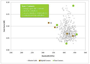
The solution is a fast, iterative AMS Reference Flow that captures all relevant variation effects into a design-specific corner based flow which represents process variation (global and local) as well as environmental variation (temperature and voltage).
Graphical data provided by Solido Design Automation‘s Variation Designer.


Comments
0 Replies to “Moore’s Law and Semiconductor Design and Manufacturing”
You must register or log in to view/post comments.