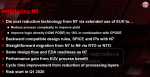
This will be a combination of the recent TSMC quarterly report, a look back at Cliff Hou’s keynote at the most recent TSMC conference, and conversations on SemiWiki.com. There has been a lot of press on this but of course the most important points are being missed. Semiconductors are complicated and getting more so, absolutely.
The big news out of the conference call was the increase in TSMC Capex from $12.5B to an even $15B which will be repeated in 2020 ($15B) and grow in 2021 due to increasing demand. Remember, TSMC closely partners with customers and builds capacity based on demand (wafer agreements) and not imagined demand like IDMS (Intel and Samsung). On the technology side lets look at the opening statement from the transcript:
C.C. Wei – Taiwan Semiconductor Manufacturing Company Limited – Vice Chairman & CEO Now I will talk about our N5 and N3 status. Our N5 technology has already entered risk production with good yield. The N5 will adopt the EUV extensively and is well on track for volume production in the first half of next year. With 80%, 8-0, logic density gain and about a 20% speed gain compared with the 7-nanometer, our N5 technology is true full node stride from our N7. We believe it will be the foundry industry’s most advanced solution with the best density, performance and power until our 3-nanometer arrives. With N5, we are further expanding our customer product portfolio and increasing our addressable market. The initial ramp will be driven by both mobile and HPC applications. We are confident that 5-nanometer will have a strong ramp and be a large and long-lasting node for TSMC.
Daniel Nenni – Founder – SemiWiki.com LLC:. 5N may be considered a full node from 7N but not 6N (with an 18% density advantage over N7). In my opinion the 6nm node will be a VERY long lasting node and while 6N revenues will be lumped into 7N and 7N+, 6N revenue will rule all, my opinion.
5N and 3N will also share the same fabs as did 10N and 7N which will again speed HVM ramp and reduce development costs. It is the TSMC recipe to foundry success, absolutely.
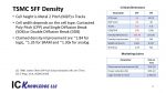
According to a conversation on SemiWiki, N5 is said to be 30nm M2P and 50nm CPP with 6 tracks and 173MTx/mm2. This works out to ~1.8x denser than N7 which is what TSMC has said. Scott Jones is pretty sure M2P is ~ 30nm and 50nm for CPP which is what is needed to get the 1.8x density improvement they have discussed.
N5P was not mentioned but from what was discussed on SemiWiki N5P is the same design rules, just more strain, a performance enhancement. Apple requires a new process every year so this is it. N5P will be out in 2021 for the Apple iProduct refresh. I would expect more optimizations will be announced next year so you may see a density improvement based on better EUV or something like that.
C.C. Wei – Taiwan Semiconductor Manufacturing Company Limited – Vice Chairman & CEO: Our N7 process is the industry’s first commercially available EUV lithography technology. N7+ provide 15% to 20% higher density with improved power consumption when compared to N7. That is already in high volume production with yield similar to N7. We expect the strong demand for N7+ continue into next year and are increasing Capex to meet this demand for multiple customers.
Now N6. Our N6 provide a clear migration path for the second-wave N7 product as its design rules are 100% compatible with N7 while providing 18% logic density gain with performance-to-cost advantage. The N6 uses one more EUV layer than N7+. N6 risk production is scheduled to begin in first quarter next year with volume production starting before the end of 2020. We reaffirm 7-nanometer will contribute more than 25% of our wafer revenue in 2019 and we expect even higher percentage in 2020 due to worldwide development of 5G, accelerated demand from HPC, mobile and other application continue to grow.
Daniel Nenni – Founder – SemiWiki.com LLC: Remember, 7N/6N is 28N déjà vu all over again so there will be plenty of 6N capacity moving forward once Apple and the other mobile giants move to 5N. The big difference between 6N and 28N is that there will be no cheap knock-off processes from UMC and SMIC, not even close.
C.C. Wei – Taiwan Semiconductor Manufacturing Company Limited – Vice Chairman & CEO Now I will talk about the N3. We are working with customers on N3 and the technology development progress is going well. Our N3 will be another full node from our N5 with PPA gain similar to the gain from N7 to N5. We expect our 3-nanometer technology will be the most advanced foundry technology in both PPA and transistor technology when it is introduced.
Daniel Nenni – Founder – SemiWiki.com LLC: TSMC N3 will again use FinFETs unlike Samsung who will use GAA which highlights the real difference between Samsung and TSMC. TSMC is focused on manufacturability versus bleeding edge technology. TSMC does not really have a choice here since they have the mobile giants (Apple, Huawei, etc…) pushing them for a new process node every year that can yield at a very high rate right out of the box. GAA will be 2nm for TSMC.
Packaging was also a focus of the call. We covered packaging and design enablement here:
A Future Vision for 3D Heterogeneous Packaging
A Review of TSMC’s OIP Ecosystem
Now for the relevant Q&A:
Gokul Hariharan – JP Morgan Chase & Co, Research Division – Head of Taiwan Equity Research and Senior Tech Analyst: So first of all, if we look at the history, whenever TSMC has had a step-up in CapEx, that is typically accompanied by a step-up in growth as well. So just wanted to kind of narrow down a little bit on the 5% to 10% growth, which is still kind of — the kind of growth that we were expecting when we were spending TWD 10 billion to TWD 11 billion. So could you give a little bit more details or maybe narrow down the forecast a little bit more for us? Because if we say a TWD 14 billion to TWD 15 billion range of CapEx, that’s closer to the high 30s or 40% capital intensity, higher than our previous range.
C.C. Wei – Taiwan Semiconductor Manufacturing Company Limited – Vice Chairman & CEO: Gokul, let me answer the question carefully. Let’s say that TSMC always build capacity, working closely with customer and to meet their demand. That’s our number one, okay? We discuss with the customer on their demand, we make our judgment also. Now we are increasing the CapEx quite a lot, no doubt about it. But then, that’s due to some of the reasons I can foresee for the future. First, the 5G’s ramp-up is much faster than 4G as we expected. Second, TSMC actually is expanding our customer portfolio, and in the same times, we’re also expanding our product portfolio. And so put all the factors together, we have a good reason that we increase our CapEx this year and probably next year.
Daniel Nenni – Founder – SemiWiki.com LLC: I was hoping packaging would come up in the Q&A. From the very beginning TSMC’s packaging efforts were looked at as a low margin business but it is also a VERY sticky business, much stickier than the wafer business. The mobile giants depend on packaging and they now “depend” on TSMC for packaging, absolutely.
Charlie Chan – Morgan Stanley, Research Division – Technology Analyst: Okay. And my next question is about the advanced packaging. I remember in the previous quarters, you commented advanced packaging should outgrow the front-end business. So first of all, is this remains the same trend? And also how about the potential margin dilution from the packaging business?
C.C. Wei – Taiwan Semiconductor Manufacturing Company Limited – Vice Chairman & CEO: The forecast on the advanced packaging business, the growth is — the growth rate is still faster than silicon growth rate. The wafer’s revenues growth rate stays the same, okay? Still that statement is still valid. The gross margin, that’s another consideration. The gross margin of the back-end business actually is lower today, still lower than the wafer margin. But we look at it whether it’s a good business to go or not on 2 factors. One, we really want to support our customer to improve their system performance. So we have to do it because of TSMC is the only one company right now who can support customers’ advanced packaging. Second actually is the CapEx intensity on the back end, and that’s advanced packaging business, is smaller. And so the asset turnover is better. So put all in all together, we still think it’s a very good business to pursue.
Daniel Nenni – Founder – SemiWiki.com LLC: As expected, the China question. TSMC’s China strategy started with Morris Chang many years ago and is nothing short of brilliant. Morris may or may not have seen the US-China trade riff coming but he positioned TSMC perfectly. TSMC has more than 400 active customers and more than 100 of those are now in China. In Q3 2019 China accounted for 20% of TSMC revenue, up from 15% last year. North America is -2% to 60%, EMEA is -1% to 6%, Asia Pacific is –1% to 9%, and Japan is -1% to 5%. I expect this trend to accelerate as the US and China continue to play economic politics.
Brett Simpson – Arete Research Services LLP – Senior Analyst: I had a question really on China. I guess in the last couple of years, we’ve seen the business double with Chinese customers. I guess at the moment, it’s pretty clear you’re going through a very healthy inflection point in the Chinese customers at the moment. So can you talk about how you see this part of the business evolving over the next 1 or 2 years? And then I guess from a planning perspective, are you concerned that the rise of your China business comes at the sacrifice of other customers, particularly U.S. companies?
C.C. Wei – Taiwan Semiconductor Manufacturing Company Limited – Vice Chairman & CEO: Well, we did see the strong course from China because that’s a very big market, especially in the semiconductor area. And we are happy to see that growth, and TSMC is offering the most leading-edge technology to support our customer in China. And so to be exact, we are going to grow with the China market. At the expense of other customer, the answer is no because we support all the customer with all our strength and our capacity.
Daniel Nenni – Founder – SemiWiki.com LLC: Interesting EUV question. I don’t remember TSMC publicly saying they made their own pellicle but of course we all knew. Yet another TSMC differentiation.
Roland Shu – Citigroup Inc, Research Division – Director and Head of Regional Semiconductor Research: Okay. And the second question is you announced that your EUV tools have been reached potentially maturity, but how about for the infrastructure? It means that for other component like photoresist, pellicle, photomask or even for this inspection tools, chemical and materials. So yes, we have — going to have a very fast ramp on 5-nanometer because of very strong demand from a customer, but are there any gating items for this EUV infrastructure will be potentially a risk?
C.C. Wei – Taiwan Semiconductor Manufacturing Company Limited – Vice Chairman & CEO: So far we do not see any gating item. All the infrastructure, actually TSMC, we are prepared. We have a — we produce our own pellicle. We have a large number of masking capacity and everything. So even photoresist, those kind of thing, we have been taking into account. So we are ready for the — actually, we are in a high-volume production for the EUV lithography technology. For next year, you have big — even higher volume, and I can assure you that we are all prepared.
C.C. Wei – Taiwan Semiconductor Manufacturing Company Limited – Vice Chairman & CEO: Okay. In TSMC, EUV lithography technology is now in the production stage. But are we happy with that? Not yet. We are still improving availability. We have output power of 250 watts, as we expected. Now we can operate the tool with 250 watts consistently. However, there’s still something that we need to improve so that we can improve the throughput, we can improve the availability so you can reduce the cost, continue to improve.
Daniel Nenni – Founder – SemiWiki.com LLC: And I’ll finish this blog with the lighter side of the Q&A. Remember this is live in front of an audience in Taipei and C.C. says this stuff with a straight face. It really is fun to watch:
Roland Shu – Citigroup Inc, Research Division – Director and Head of Regional Semiconductor Research: Okay. I think just a follow-up for — I know you don’t comment on the ASP, but for the same amount of the wafer shipment on N7+, is this going to contribute more revenue upside to TSMC?
C.C. Wei – Taiwan Semiconductor Manufacturing Company Limited – Vice Chairman & CEO: You just mentioned we don’t.
Roland Shu – Citigroup Inc, Research Division – Director and Head of Regional Semiconductor Research: No, I talk about revenue. I don’t talk about ASP.
C.C. Wei – Taiwan Semiconductor Manufacturing Company Limited – Vice Chairman & CEO: That’s the same thing.
Bruce Lu – Goldman Sachs Group Inc., Research Division – Research Analyst: That’s why I wanted you to give us some hint, right? We cannot just tell my investors that we have to trust TSMC. Even though I say that all the time but…
C.C. Wei – Taiwan Semiconductor Manufacturing Company Limited – Vice Chairman & CEO: You can trust TSMC. No doubt about it.
Daniel Nenni – Founder – SemiWiki.com LLC: Absolutely!
Reference: https://www.tsmc.com/uploadfile/ir/quarterly/2019/3d36C/E/TSMC%203Q19%20transcript.pdf