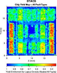
Yield, no topic is more important to the semiconductor ecosystem. After spending a significant part of my career on Design for Manufacturability (DFM) and Design for Yield (DFY), I’m seriously offended when semiconductor professionals make false and misleading statements that negatively affects the industry that supports us.
TSMC’s 28-nm process in trouble, says analyst – Mike Bryant, technology analyst with Future Horizons Ltd. has said that foundry Taiwan Semiconductor Manufacturing Co. Ltd. is in trouble with its 28-nm manufacturing process technologies, which are not yet yielding well. Bryant referenced un-named contacts made with multiple companies waiting for designs to be produced by TSMC on 28-nm processes. Bryant said that there are 10 designs in manufacture from seven companies. “We’re now hearing none of them work; no yield anyway,”
Xilinx Reaches Industry Milestone with Record-Fast 28nm Product Rollout
The “this foundry is not yielding at a specific process node” comments posted on the Web by journalists and analysts, who should know better, not only offend me, they also insult TSMC and TSMC’s top customers who ARE yielding. If you are going to talk authoritatively about semiconductor yeild you should at least know that the path to production for a given device is a combination of “process-limited yield” and “design-limited yield”.
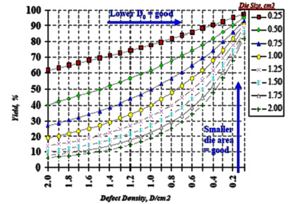
Traditional models for process-limited yield are based upon random defect fails, and have stood the test of time over many process generations. The size and density of particulate and lithographic defects is continuously monitored, using visual and electrical measurements taken on specific non-design structures. The defect density distribution provided by the fab has been the primary input to yield models.
When the fab states, “We have achieved a random defect density of D < x / cm**2 on our process qualification ramp.” (where x << 1), this measure is indicative of a level of process-limited yield stability. The design team incorporates this input with their measures of the “critical area analysis”, to estimate the resulting manufacturing yield.
Qualcomm Announces Next-generation Snapdragon Mobile Chipset Family
There are parametric yield loss factors as well, which relate to the electrical characteristics of devices and parasitics. These parameters are monitored using electrical measurements taken on additional non-design structures during fabrication – excursions of these parameters outside process model limits will limit the design from meeting electrical specifications. The cost assumptions made by design teams typically focus on random defect-limited yield.
 As the semiconductor industry entered the era of sub-wavelength resolution, designers learned of the “resolution enhancement technology” algorithms that were being applied by the mask house. Fabrication design rules were augmented to include “recommended”, then “restricted”, and now “equation-based” specifications to enhance the window of process variation latitude.
Yet, as the fabrication industry continues on the aggressive schedule for subsequent process nodes continuing to use 193nm wavelength exposure – 32nm, 28nm, 22nm, 20nm, 14nm – it is no longer possible to capture all the the fabrication process and layout interactions in a set of design rule checks.
Altera Unveils Innovations for 28-nm FPGAs
Bottom line: Design teams today must accept a greater responsibility for the product-specific yield. As a result, addressing “design-limited yield” factors is now a critical pre-tapeout requirement.
The “best” approach toward improving design-limited yield starts at the design planning stage. For those design companies that develop IP, there are numerous design-for-yield vs. area/performance tradeoffs that need to be addressed – e.g., the transistor gate pitch dimension, circuit nodes with multiple contacts, or the use of larger rectangular contacts, the addition of dummy devices, and the pin geometry for connectivity. At higher levels of IP integration, the choice of the wiring track dimensions for routing and power grid distribution and via insertion has a major impact upon the design-limited yield.
Bottom line: The design teams that collaborate with the fab to better understand how to make design-limited yield tradeoffs in initial planning and near tapeout will have a much smoother path toward realizing product revenue and margins.
Oracle Plans to Speed Up Release of Next-Generation 28nm SPARC T5 Chip
The EDA industry has assisted design teams with addressing process-limited and design-limited yield by offering products for DFM and DFY. These terms are often used synonymously, although in the same sense that there are different yield responsibilities, these terms are also very different.
Yet, the most important design-limited yield issues don’t need EDA tool support – they are addressed DURING initial design planning. So, the next time you hear someone say, “that process is not yielding…”, be sure to stop them and ask: “Are you sure? What are the process-limited and design-limited yield issues?”
Or you can try a more direct approach and ask: Why are other companies yielding at TSMC 28nm and you are not?


Comments
0 Replies to “TSMC 28nm Yield Explained!”
You must register or log in to view/post comments.