As you’ve probably seen in (excellent!) recent semiwiki postings by Eric Esteve and Scotten Jones, 12nm FD-SOI has now officially joined the GlobalFoundries’ roadmap. Eric and Scotten did a great job of putting many things in perspective. But this is a big piece of news, so here I propose looking at it from yet another perspective,… Read More

Intel Altera FPGA at the heart of an autonomous Audi A8
Audi announced its piloted driving technology at CES 2015. The Audi Prologue includes the Advanced Driver Assistance System Platform (zFAS), co-developed with TTTech. The zFAS board is based on four devices: an Nvidia k1 processor and Infineon Aurix processor, Mobileye’s EyeQ3 for vision processing, and an Altera Cyclone … Read More
Will TSMC be alone at 10nm and 7nm?!?!?
Now that the dust has settled let’s talk about the recent TSMC OIP Ecosystem Forum. This was the 6[SUP]th[/SUP] annual OIP which hosts more than 1,000 attendees from TSMC’s top customers and partners. Presenting this year were TSMC VP and CTO Dr. Jack Sun, TSMC VP of R&D Dr. Cliff Hou, and ARM EVP of Incubation Businesses Dr. Dipesh… Read More
Intel Foundry Rounds Out IP Lineup With ARM at IDF 2016
There are always debates on who does what best in the semiconductor industry, but most agree that Intel is the best in process and transistor technology. This leadership has served the company extremely well over the last few decades and allowed them to reach a position of dominance in the PC and server semiconductor markets. In … Read More
What Will Kill ROP Cyberattacks?
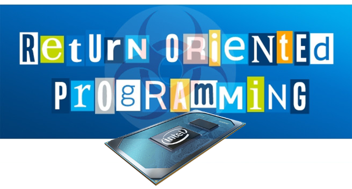
IBM recently announced a software-oriented solution to help eradicate Return Oriented Programming (ROP) malware attacks. ROP is a significant and growing problem in the industry. Crafty hackers will use snippets of code from other trusted programs and stitch it together to create their attacks. It has become a very popular… Read More
The Status and Future of FDSOI
I recently took a look at the current status and future direction of FinFET based logic processes in my Leading Edge Logic Landscape blog. I thought it would be interesting to take a similar look at FDSOI and to compare and contrast the two processes. My Leading Edge Logic Landscape blog is available here.… Read More
Top 5 Highlights from the 2016 TSMC Open Innovation Platform Forum
Recently, TSMC conducted their annual Open Innovation Platform forum meeting in San Jose. Although TSMC typically eschews a theme for the forum, David Keller, EVT TSMC North America, used a phrase in his opening remarks that served as a foundation for the rest of the meeting – “celebrate the way we collaborate”.
The forum begins… Read More
ESL Architectural Power Estimation Support from TSMC — yes, TSMC
Electronic system level (ESL) modeling for system architecture exploration is rapidly gaining momentum. The simulation performance requirements for hardware/software co-design are demanding — an abstract model for SoC IP cores is required. Typically, soft IP will include a number of model configuration parameters.… Read More
GLOBALFOUNDRIES Extends the FDSOI Roadmap
On September 8, 2016 GLOBALFOUNDRIES (GF) announced their 12nm FDSOI technology node. On September 12th I had a chance to interview Greg Bartlett, GF Senior Vice President for the CMOS Business Unit (as a side note, GF has: RF SOI, ASIC and CMOS business units).… Read More
FREE Fabless: The Transformation of the Semiconductor Industry!
As most of you know SemiWiki published a book which is a really nice history of the fabless semiconductor ecosystem. Thousands of people have copies, we have received many compliments on it, and we are very proud. As a thank you to all SemiWiki members I would like to offer a free electronic version of the book (PDF). You can access it… Read More
TSMC CoWoS versus Intel EMIB Semiconductor Packaging