Although there has been always a strong relationship between ARM and GlobalFoundries, it is interesting to notice that Intel has helped to boost it and make it even stronger. Indeed when AMD renegotiated its x86 licensing deal with Intel in 2009, one of the most significant long-term changes was a marked reduction in how much of GlobalFoundries AMD had to own in order to remain within the terms of its manufacturing license. As a result of this change, AMD announced in January 2010 that it intended to significantly accelerate the financial split between itself and GlobalFoundries; we now have seen the impact of that transition on the GlobalFoundries’ side of the business. During 2010, GFI has developed a new strategic partnership with ARM, in which the two companies collaborate on leading-edge, 28nm system-on-chip (SoC) designs. This strategy should allow GlobalFoundries to attract more customers especially this designing Application processor for the wireless handset segment. We have to keep in mind that the Smartphone market has been 302 Million unit in 2010 with a 70% YoY growth rate (and is expected to grow to about 600 Million in 2015) to be compared with a total PC market at 350 Million where Intel processors represent 80% market share, leaving a TAM of 70 Million units for their competitor, and the foundries processing the processor. We now better understand how strategic is for GlobalFoundries such a move to enhance ARM partnership, and be the first to support ARM Cortex A9 in 28nm.
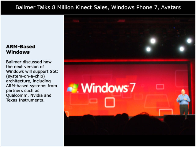
ARM Processor IP strengths are well known: for a similar performance level, ARM-based chip power consumption will be 50% less than for Intel IC, the figures for standby power being better by a factor up to ten, but this highly depend of the chip maker know how in term of power management. One weakness of ARM architecture, the lack of Microsoft support, is expected to quickly vanish, as Microsoft has announced during 2011 CES the support of “SoC architecture, including ARM based systems”. This evolution is more like a revolution, as it is the first time since the 20 years ARM architecture is available!

Globalfoundries has decided in 2009 to be the first foundry to work with ARM to enable a 28nm Cortex-A9 SoC solution. The SoC enablement program, built around a full suite of ARM Physical IP, Fabric IP and Processor IP, will deliver customers advanced design flexibility. The collaborative efforts of the partnership will initially focus on enabling SoC products which use the low power and high performance ARM Cortex -A9 processor on Globalfoundries 28nm HKMG process.

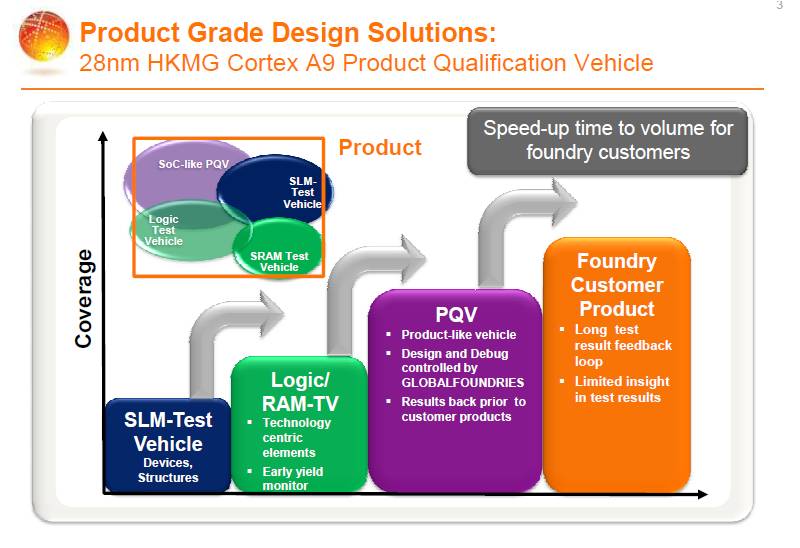
Looking at the flow allowing to speed-up time to volume for foundry customers, we see that the last milestone is develop, process and characterize the Product Qualification Vehicle (PQV). In this case, the jointly developed Test Qualification Vehicle (TQV) reached the tapeout stage in August 2010 at GLOBALFOUNDRIES Fab 1 in Dresden, Germany. If we look at the different building blocks part of this TQV: Std Cells, I/O, Memory, the Cortex A9 core and some market specific IP like USB, PCIe or Mobile DDR Controller, you see that all of these allow to build a product grade SoC. When this PQV has been tapeout then processed, running the validation on the Silicon samples will allow to do data correlation, improving the accuracy of the models used by the designers of “real” products.

The TQV will be based on GLOBALFOUNDRIES 28nm High Performance (HP) technology targeted at high-performance wired applications. The collaboration also will include the 28nm High Performance Plus (HPP) technology for both wired and high-performance mobile applications, and the Super Low Power (SLP) technology for power-sensitive mobile and consumer applications. All technologies feature GLOBALFOUNDRIES’ innovative Gate First approach to HKMG. The approach is superior to other 28nm HKMG solutions in both scalability and manufacturability, offering a substantially smaller die size and cost, as well as compatibility with proven design elements and process flows from previous technology nodes. If we want to compare the same Cortex A9 based chips, these built using 28nm HKMG from GlobalFoundries will deliver a 40% performance increase within the same thermal envelope as 40- or 45-nm products. Coupling their know-how, ARM and GlobalFoundries also say they can achieve up to 30% less power consumption and 100% higher standby battery life.

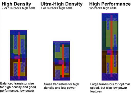
As you can see on this figure from ARM, a design team always can optimize the core instantiation in respect with the application, and the desired performance to power trade-off, by selecting the right library type. He can also design, within the same chip, some specific blocks targeting high speed by using the 12-tracks high cells, when the rest of the chip will be optimized for power consumption at first (if the target application is battery powered) or for density, when the target application require the lowest possible unit price. Having these libraries and processor IP from ARM available on various process nodes and variants (like HP, HPP and SLP in 28nm HKMG) is key for the semiconductor community –the fables and also the IDM who adopt more and more a “fab-lite” profile.
Because the layout picture of a device tells more than a long talk (and also because that’s remind me the time where I was an ASIC designer), I cannot resist and show you the layout of the Cortex A9 based TQV device:

Eric Esteve (eric.esteve@ip-nest.com)


Captain America: Can Elon Musk Save America’s Chip Manufacturing Industry?