TSMC recently held their Open Innovation Platform (OIP) Ecosystem Forum event where many of their key partners presented on their latest projects and developments. This year one of their top IP provider partners, Analog Bits, gave two presentations. Analog building blocks have always been necessary as enabling technology on leading edge designs. The move to 3nm continues this important relationship. Analog Bits has developed specialized analog IP that can help differentiate end products. For instance, they have focused on optimized high performance and low power SerDes, among other things. Another significant area is specialized on-chip sensors for monitoring chip health and performance.
In his presentation Mahesh Tirupattur, Analog Bits’ EVP, discussed how their sensing IP was used by Cerebras in developing the largest chip ever designed. The Cerebras WSE-2 has 2.6 trillion transistors in 850,000 optimized cores covering 46,225 square mm of silicon. Cerebras faced challenges in power distribution and power supply integrity. Analog Bits IP offered them a solution to monitor chip operation in real time that can be used to apply real time corrective actions. They used 840 distributed glitch detectors to provide real time coverage of the entire design. The Analog Bits glitch detectors can detect short duration events that could otherwise easily be missed. They are programmable for trigger voltage, depth of glitch and time span of glitch. Their sensitivity exceeds 5pVs.
Recently Analog Bits expanded their sensor offering by adding power supply glitch detectors with an integrated voltage reference to their lineup of integrated POR sensors and on-die PVT sensors. This allows them to cover all aspects of chip operation in real time, including POR conditions – and now the health of the power supplies.
Of course, sensors require extremely high accuracy to correctly report chip behavior. Similarly, clocking macros need accuracy to enable proper chip operation. So, it was good to see that their second presentation at OIP was specifically on the topic of design and verification of these blocks. The paper was titled “Design and Verification of Clocking Macros and Sensors in N5 and N3 Processes Targeting High Performance Compute, Automotive, and IoT Applications”, and authored by Sweta Gupta, Director of Circuit Engineering at Analog Bits and Greg Curtis, Sr. Product Manager of Siemens EDA. The paper itself was the result of a three-way collaboration between TSMC, Siemens and Analog Bits.
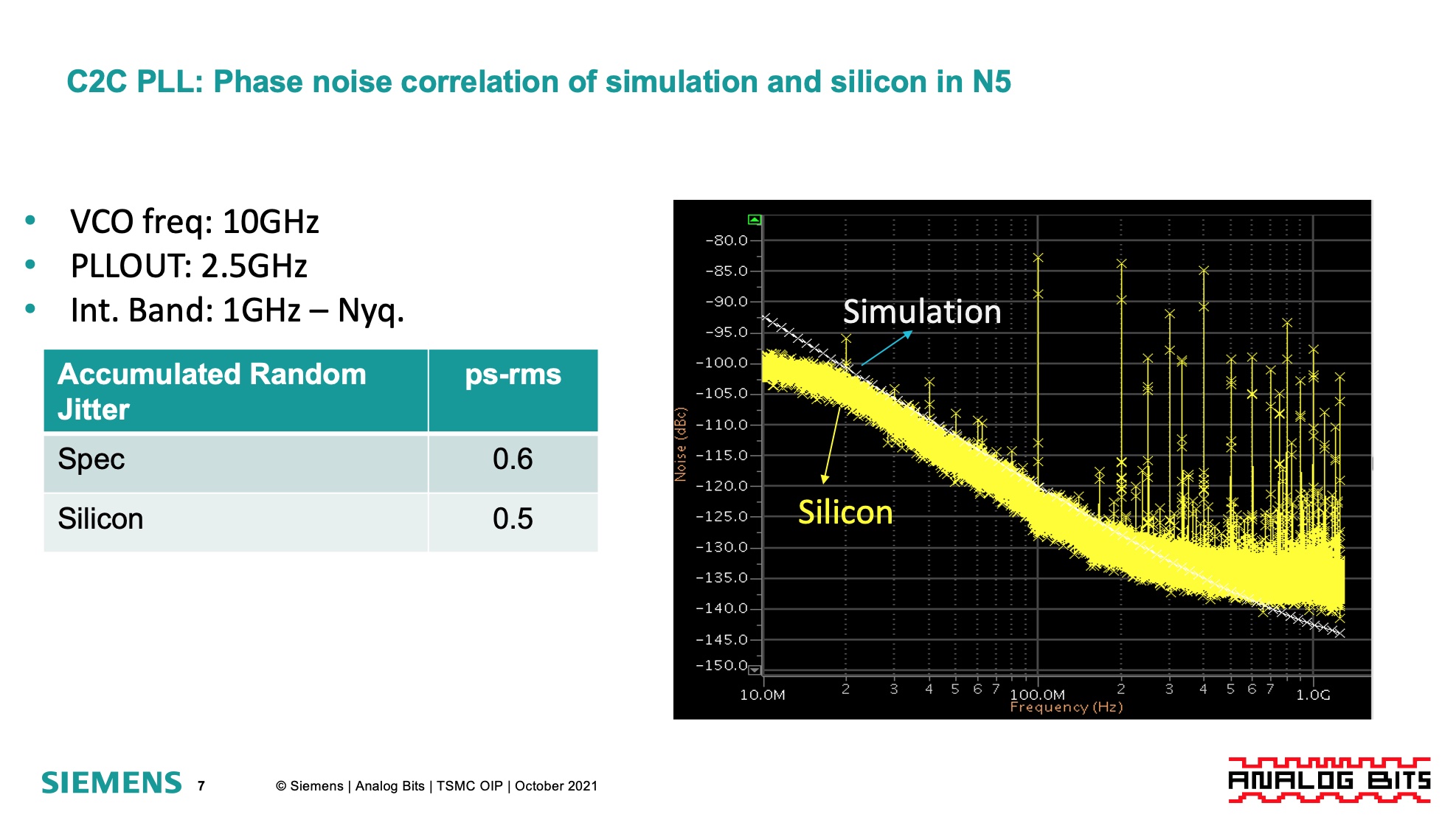
In the second presentation Analog Bits shared correlation data on silicon measurements to specification for several of their PLLs, a power supply droop detector and a temperature sensor. Here is one of their slides on the phase noise correlation between measurement and silicon for a PLL built in TSMCs N5.

Analog Bits has a broad and well thought out portfolio of analog IP. They have customers on a wide range of processes from 0.25um to 3nm. I am sure that part of their success stems from their no-royalty business model. They have billions of units shipped from over a thousand IP deliveries since they first started in 1995. While the OIP presentations are over, more detailed information on all of their IP for on-chip sensors, SerDes, clocks and I/Os is available by contacting them. Their website offers detailed products listings & data sheets, and access to their N5 test chip video.
Also read:
Package Pin-less PLLs Benefit Overall Chip PPA
Analog Sensing Now Essential for Boosting SOC Performance
Analog Bits is Taking the Virtual Holiday Party up a Notch or Two
Share this post via:


Comments
There are no comments yet.
You must register or log in to view/post comments.