Spacer-defined patterning is an expected requirement for advanced semiconductor patterning nodes with feature sizes of 25 nm or less. As the required gaps between features go well below the lithography tool’s resolution limit, the use of cut exposures to separate features is used more often, especially in chips produced by TSMC or Intel, where “cut poly” and “cut metal” are applied [1,2]. However, line cutting introduces new concerns, such as placement error as illustrated in Figure 1.

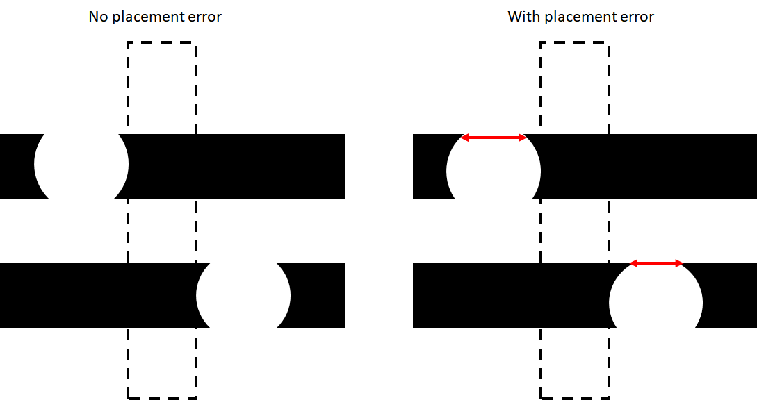
Figure 1. The effect of line cut placement error is to increase the risk of arcing across the narrowest portion of the gap (right).
The cut itself is expected to be round when confined to very small spaces. These will lead to burrs or spurs at the cut locations. Moreover, the cut itself cannot be perfectly placed all the time, and this leads to the spurs narrowing the gap toward one side. Consequently, unwanted arcing across the gap is likely. Fortunately, there are a number of ways to address this issue today.
Solution 1: Design rule/layout restrictions
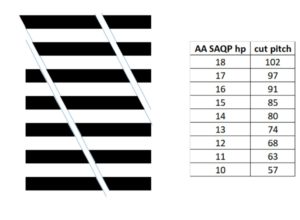
The quickest way to avoid these issues is to have enough clearance for the cuts not to be rounded. This would mean the layout of Figure 1 with the gaps close to one another would become forbidden as part of the Design Rule Check (DRC) violations [2]. On the other hand, some layouts such as DRAM active area (see Figure 2 for example) are more tolerant.

Figure 2. The cut for the DRAM active area shown here (18.4 degrees from vertical) is achievable by immersion single exposure with a phase shift mask for features<0.5 wavelength/NA[3], for cut pitches of 80 nm and above. For smaller cut pitches, double patterning, e.g., spacer double patterning, would be required.
Solution 2: Cut grid with selection mask
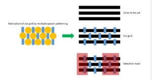
If the layout of Figure 1 must be used, then a different process must be used to ensure a straight edge cut. One possible approach is to use a cut grid with a selection mask[4]. This is illustrated in Figure 3.

Figure 3. Process sequence for cut selection from a pre-defined cut grid.
This particular approach would entail that the cut would require three masks instead of one. The first two masks would define the cut grid in an etch mask over the pre-patterned lines. The first mask would define a grid of lines perpendicular to the lines to be cut, and a second mask would define posts where the rectangular target cut locations would be separated. A third mask would select the actual cut locations from the grid. The advantage of the cut selection approach is that the cut grid is already predefined with straight edge cuts. However, it does require more masks and process steps.
Solution 3: Self-aligned blocking (or cutting)
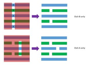
A reduction of masks is possible with the self-aligned blocking (SAB) approach [5]. In this approach, the spacer-defined lines are divided into two groups in an ABAB.. fashion, where any two adjacent lines separated by spacers belong to different groups (A or B). Two different materials in the process flow are used to represent each group (Figure 4). These two materials are selected so that one may be etched without affecting the other. The spacers in between the two materials are also not etched. Consequently, a cut across five lines may cut the two selected lines with the straight edge allowed by the longer length of the cut. There is one cut mask for removing A material only and one for removing B material only. Note that the cut masks may also make use of spacer-defined double patterning [6]. The emergence of SAB means that two masks (for A and B) will be used independently of wavelength.

Figure 4. Self-aligned blocking (or cutting) approach makes use of etch selectivity to avoid unwanted cutting of adjacent feature lines.
References
[1] M. C. Smayling, V. Axelrad, “Simulation-Based Lithography Optimization for Logic Circuits at 22nm and Below,” SISPAD 2009.
[3] L. W. Liebmann, J-A. Carballo, “Layout Methodology Impact of Resolution Enhancement Techniques,” Proc. 2003 Intl. Symp. Phys. Design, 110.
[4] http://www.tela-inc.com/wordpress/wp-content/uploads/2012/05/SPIE-2013_8683.pdf
[6] US Patent 9240329, assigned to Tokyo Electron Limited, filed Feb. 17, 2015.
Share this post via:


Facing the Quantum Nature of EUV Lithography