Extreme ultraviolet (EUV) lithography targets sub-20 nm resolution using a wavelength range of ~13.3-13.7 nm (with some light including DUV outside this band as well) and a reflective ring-field optics system. ASML has been refining the EUV tool platform, starting with the NXE:3300B, the very first platform with a numerical aperture of 0.33. With the current NXE:3400B platform, a pupil fill ratio lower limit of 20% (without loss of light) is now possible, offering improved contrast for smaller features [1]. In this article, the basic reasons behind this improvement are presented.
Illumination locations in the pupil
The pupil is essentially an aperture or window through which the specified angles of illuminating the EUV mask go through. The center angle is along the optical axis, which naturally folds throughout a reflective optical system, and also happens to be at a 6 degrees with respect to the normal to the mask. A pupil can be represented as an assembly of points, whose x and y coordinates are the sine of the angle made with the optical axis in x and y directions, respectively.
Optical projection systems basically operate on spatial frequencies, which in turn are indicators of feature pitches (spatial frequency = 1/pitch). Images containing larger pitches, more isolated features, will have a wide range of spatial frequencies, including very low ones. Images containing the densest features, smallest pitches, will have only the highest spatial frequencies. When the spatial frequency is too high, it will be cut off by the numerical aperture of the final lens (or mirror in the case of EUV). The numerical aperture is essentially a low-pass filter. In order to retain these high spatial frequencies, it would be necessary to shift the illumination, selecting pupil points which are off-center. This shifts the target spatial frequencies away from the cutoff edge of the numerical aperture.
Stochastic Effect of Large Pupil Fill
Complex 2D patterns will contain both minimum pitches and much larger pitches. In that case, it is necessary to check each point in the pupil for what images will result from an illumination from that point.
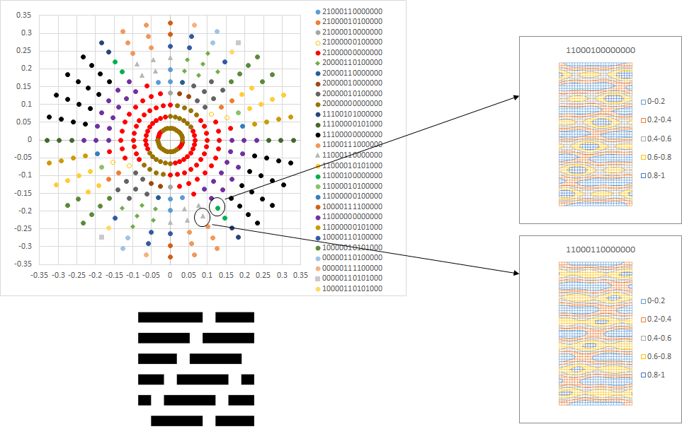
Figure 1 shows an example for where minimum pitch is 28 nm, and there are larger pitches of 84 nm in x and 168 nm in y. The wavelength is taken to be 13.5 nm, the numerical aperture to be 0.33.
Figure 1. Images from two different neighboring source points in the pupil. The target pattern is on the lower left. Although quite similar, the two images are distinctly different. In a realistic exposure condition, both would be represented by very small fractions of the total dose.
The images produced by two neighboring source points were shown to be similar but still different. Assuming a conventional illumination condition with sigma=1 (maximum on NXE:3400B [2]), uses the entire displayed collection of source points, and represents the largest possible pupil fill. Under this condition, the images represented by these two selected source points are only supported by 1-3% of the dose applied at the wafer. Hence there are few photons emanating from these points (<1 mJ/cm2, <1 photon/nm2), which aggravates the shot noise.
If fewer differently diffracted images need to be added up together to form the final image, this would reduce the stochastic impact. Presumably, instead of the conventional illumination using all the displayed points, only a certain optimized subset would work. This is the basic principle behind source-mask optimization (SMO) [3]. Naturally, the pupil fill is thus reduced. Ideally, only one diffracted image will be used, with all the exposure dose going there. However, the pupil fill fraction may go very low, even as low as 1-3% if we used one of the two source points used above as examples. On the current NXE:3400 systems, pupil fill fractions below 20% will result in loss of throughput [2].
Rotation Sensitivity for Dense Features
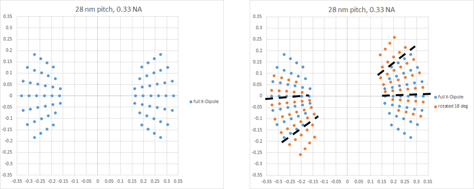
For a 0.33 NA and central wavelength of 13.5 nm, dense features with pitches of 40 nm or less can only be resolved by illuminations at wide enough angles, i.e., angles that deviate far enough from the optical axis. As an example, a 28 nm vertical line pitch can only be resolved by a distribution of angles indicated by the blue dots in the left part of Figure 2.
However, since the EUV optical system is reflective, it requires a ring-field to minimize aberrations. This, in turn, requires the exposure field to be shaped like an arc. The pupil is rotated azimuthally through this arc across the field, in some reported cases by over 24 degrees [4, 5].
Figure 2. Left: Dipole illumination for 28 nm vertical line pitch. Right: after 18 degree rotation at a different slit position, some illumination points are outside the originally allowed range. This would lead to more background light washing out the image. A reduced pupil fill (including points only within the dotted lines) avoids this outcome.
The right part of Figure 2 compares the original illumination distribution with after an 18 degree rotation. Some points in the original illumination distribution have now been rotated outside into the forbidden illumination zone. These illumination points will now degrade the final image, as they no longer let the required spatial frequencies pass through to the wafer. They only contribute background light. Hence, to avoid this, a subset of the original distribution (marked by the dotted lines) should be used. However, this pupil fill will be less than 20%.
Alternatively, to use a larger pupil fill, the rotation range can be reduced by limiting the field width [6]. Instead of the full 26 mm width of the exposure field, half of it or less can be used instead. The tradeoff here is that the scanner now must make more exposure field stops across the wafer, and this also limits throughput.
Conclusions
The need for pupil fill reduction can now be understood as conferring benefits of reduced impact from stochastics and pupil rotation in EUV lithography. However, with the likely need to go to pupil fill ratios of <20%, throughput concerns cannot be ignored.
References
[1] A. Pirati et al., Proc. SPIE 9776, 97760A (2016).
[2] M. van de Kerkhof et al., Proc. SPIE 10143, 101430D (2017).
[3] A. E. Rosenbluth et al., Proc. SPIE 4346, 486 (2001).
[5] R. Capelli et al., Proc. SPIE 10957, 10950X (2019).
This article first appeared in LinkedIn Pulse: The Need for Low Pupil Fill in EUV Lithography


Musk’s Orbital Compute Vision: TERAFAB and the End of the Terrestrial Data Center